Mtj manufacturing method utilizing in-situ annealing and etch back

a manufacturing method and in-situ annealing technology, applied in the field of magnetic memory elements, can solve the problems of preventing the advancement of the use of mtjs, the current and threshold voltage requirements are currently too high to allow practical applications of the spin transfer torque based mtj, and the mtjs exhibit a considerable low stiffness

a manufacturing method and in-situ annealing technology, applied in the field of magnetic memory elements, can solve the problems of preventing the advancement of the use of mtjs, the current and threshold voltage requirements are currently too high to allow practical applications of the spin transfer torque based mtj, and the mtjs exhibit a considerable low stiffness

US20140248719A1Active Publication Date: 2014-09-04AVALANCHE TECH

Image

  • Mtj manufacturing method utilizing in-situ annealing and etch back
  • Mtj manufacturing method utilizing in-situ annealing and etch back
  • Mtj manufacturing method utilizing in-situ annealing and etch back

Examples


Embodiment Construction

[0019]In the following description of the embodiments, reference is made to the accompanying drawings that form a part hereof, and in which is shown by way of illustration of the specific embodiments in which the invention may be practiced. It is to be understood that other embodiments may be utilized because structural changes may be made without departing from the scope of the present invention. It should be noted that the figures discussed herein are not drawn to scale and thicknesses of lines are not indicative of actual sizes.

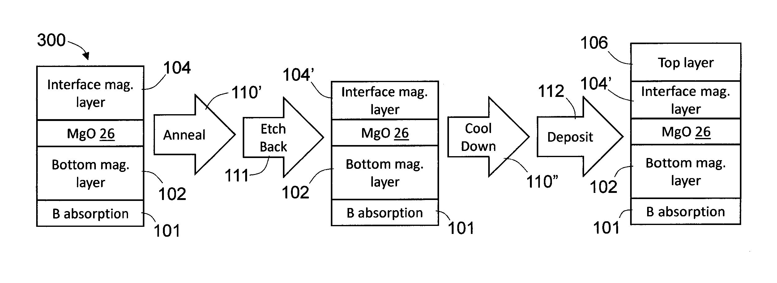
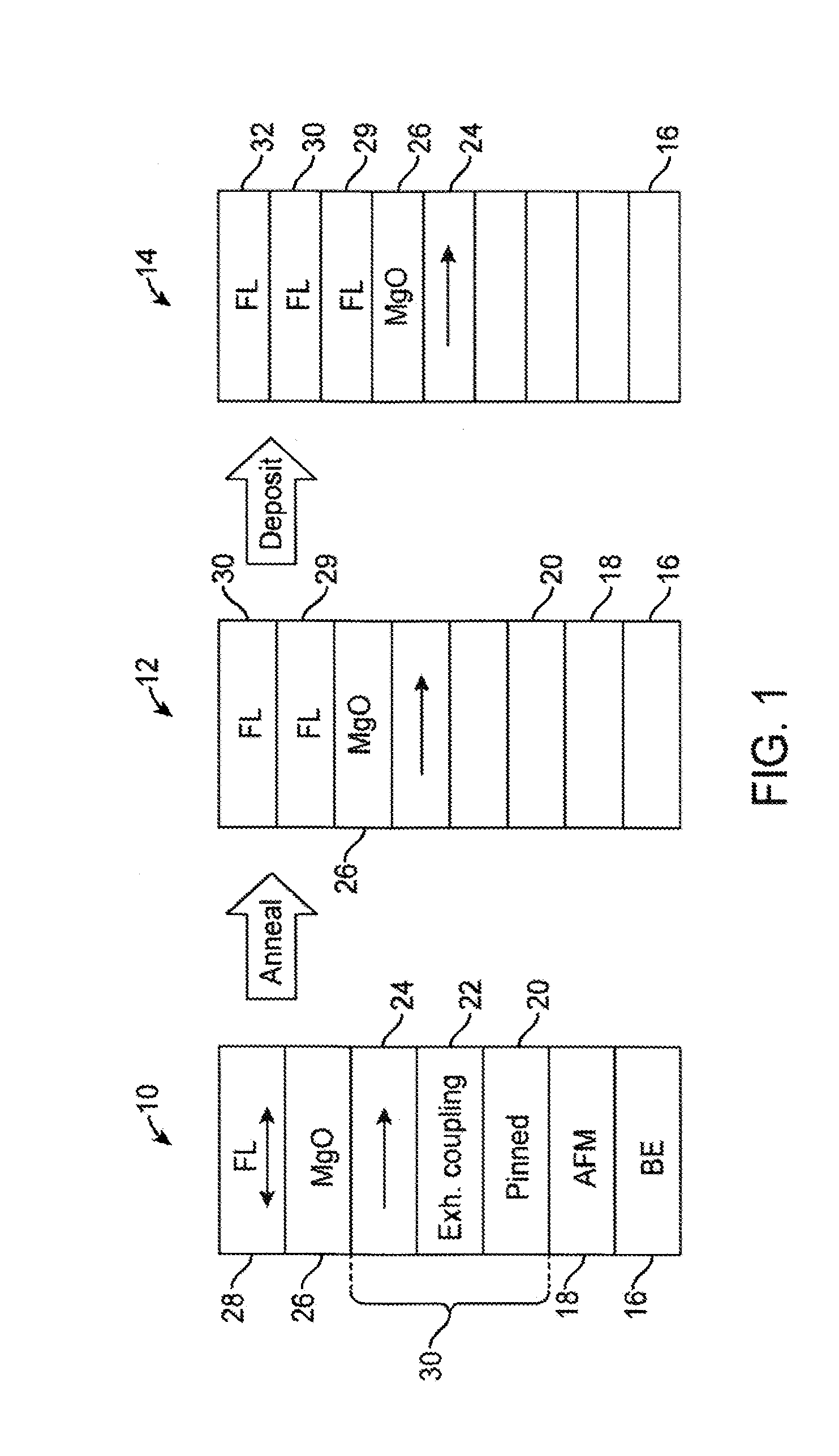
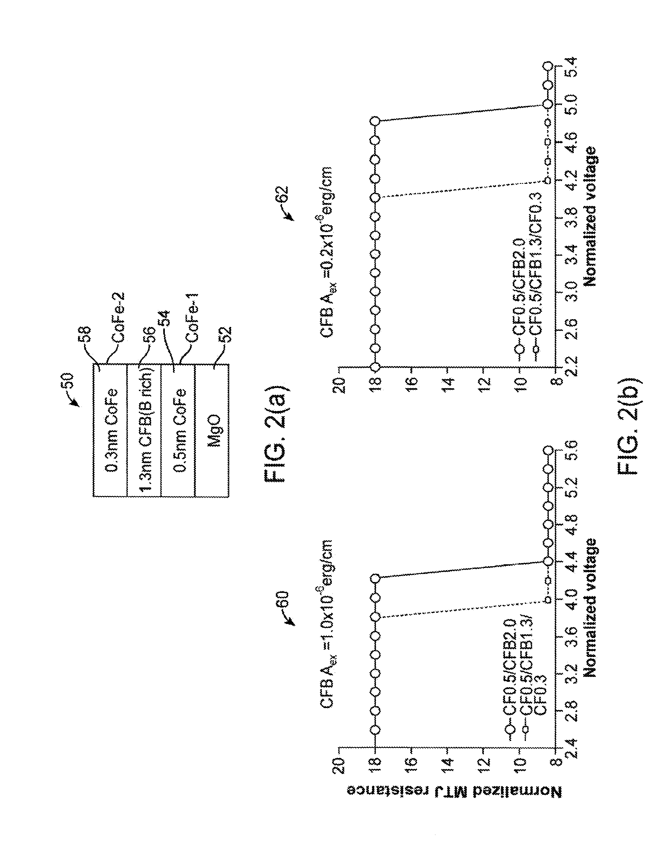
[0020]In an embodiment of the present invention, a spin transfer torque magnetic random access memory (STTMRAM) element and a method of manufacturing the same is disclosed. Relevant layers of the STTMRAM element include a free layer structure, having enhanced internal stiffness, and made of sub-layers using an annealing process. In forming the free layer structure, a first free layer is deposited on top of a barrier layer, the first free layer being made p...


PUM


Abstract

The present invention is directed to a method for manufacturing spin transfer torque magnetic random access memory (STTMRAM) devices. The method, which utilizes in-situ annealing and etch-back of the magnetic tunnel junction (MTJ) film stack, comprises the steps of depositing a barrier layer on top of a bottom magnetic layer and then depositing an interface magnetic layer on top of the barrier layer to form an MTJ film stack; annealing the MTJ film stack at a first temperature and then cool the MTJ film stack to a second temperature lower than the first temperature; etching away a top portion of the interface magnetic layer; and depositing at least one top layer on top of the etched interface magnetic layer. The method may further include the step of annealing the MTJ film stack at a third temperature between the first and second temperature after the step of depositing at least one top layer.

Description


Claims


Application Information

Patent Timeline
04 Sep 2014
Publication
US20140248719A1