
Dual data rate bridge controller with one-step majority logic decodable codes for multiple bit error corrections with low latency

a bridge controller and data rate technology, applied in error detection/correction, redundant data error correction, instruments, etc., can solve problems such as affecting multiple memory bits, affecting the overall system performance, and induced errors

Inactive Publication Date: 2014-09-18
AVALANCHE TECH
View PDF3 Cites 6 Cited by
  • Summary
  • Abstract
  • Description
  • Claims
  • Application Information

AI Technical Summary

Benefits of technology

The present invention provides methods for multiple bit error tolerant memory modules that can be integrated into current and next generation memory subsystems. The invention includes a bridge controller that performs multiple-bit error detection and correction on data stored in the memory components. The invention also includes a non-volatile memory subsystem and a data format element, as well as timing diagrams for read and write operations. The technical effects of the invention include improved data reliability and durability, reduced latency, and improved performance and efficiency of memory subsystems.

Problems solved by technology

Multiple-bit error correction codes are difficult to implement and consume many clocks of latency thereby degrading the overall system performance.
As technology scales to nanometer granularity, induced errors will impact multiple memory bits.

Method used


Image

  • Dual data rate bridge controller with one-step majority logic decodable codes for multiple bit error corrections with low latency
  • Dual data rate bridge controller with one-step majority logic decodable codes for multiple bit error corrections with low latency
  • Dual data rate bridge controller with one-step majority logic decodable codes for multiple bit error corrections with low latency

Examples


Embodiment Construction

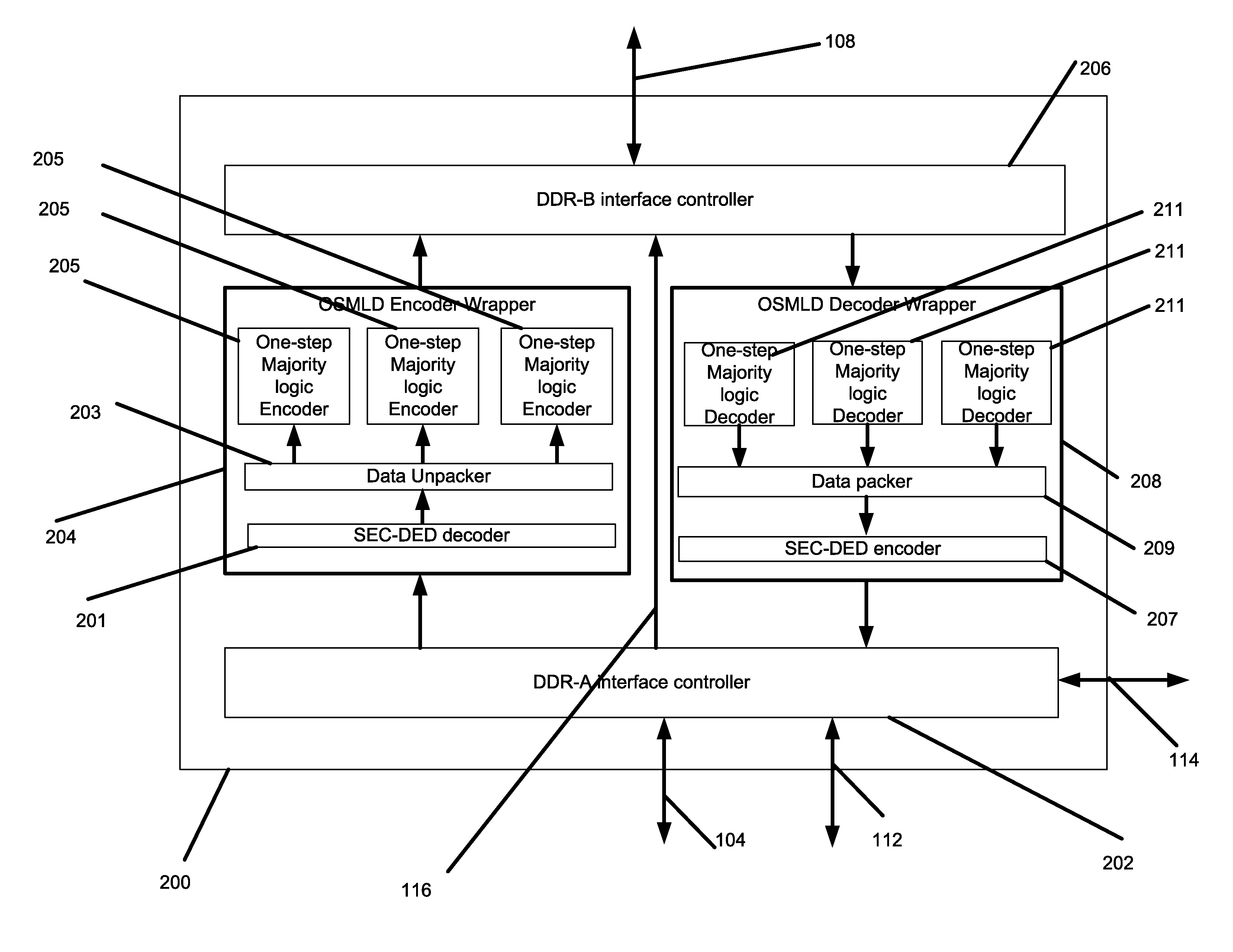
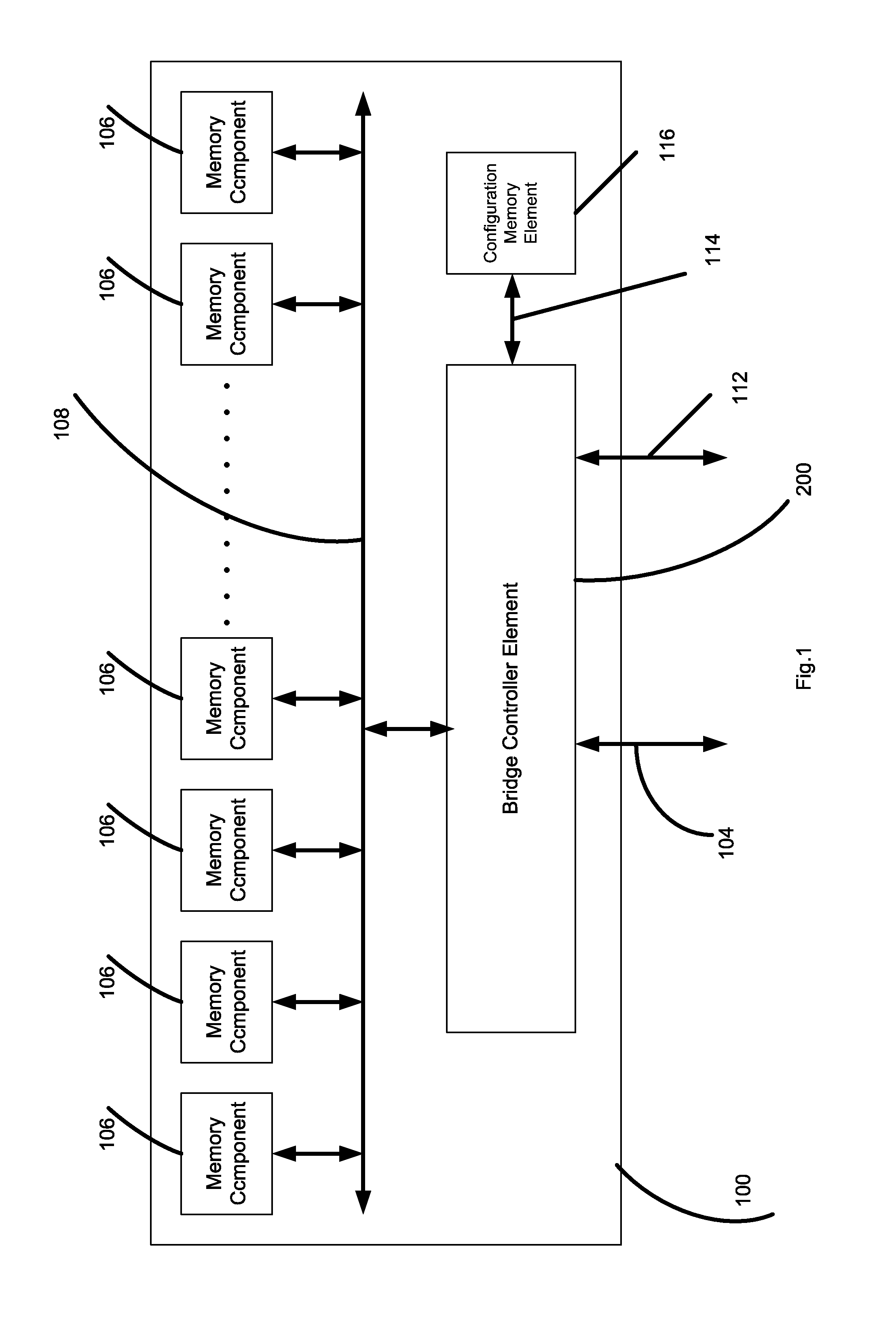
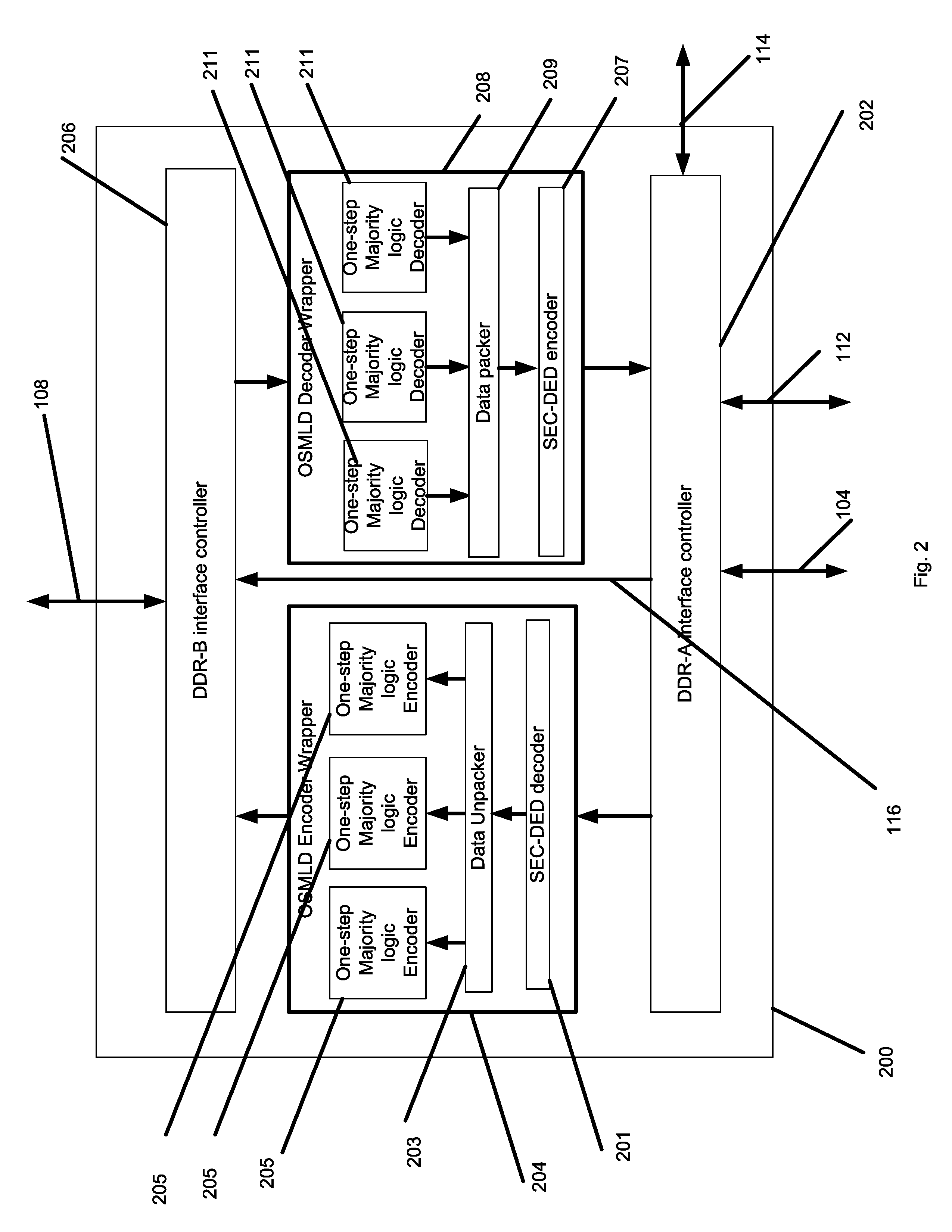
[0020]In the following description of the embodiments, reference is made to the accompanying drawings that form a part hereof, and in which is shown by way of illustration of the specific embodiments in which the invention may be practiced. It is to be understood that other embodiments may be utilized because structural changes may be made without departing from the scope of the present invention. It should be noted that the figures discussed herein are not drawn to scale and thicknesses of lines are not indicative of actual sizes.

[0021]In accordance with an embodiment of the invention, a memory module refers to an array of memory components, passive and active components and a bridge controller with an ability to process the data stream. Each memory component stores the data without any modifications to the input data stream and includes core and peripheral circuits, row and column decoders, sense amplifiers and the like. Bridge controller can be either a programmable device or an ...


PUM


Abstract

A memory module includes a bridge controller having a first interface and a second interface. The first interface receives commands and data from a host and the second interface is coupled to one or more memory components. The bridge controller performs multiple-bit error detection and correction on data stored in the one or more memory components.

Description

CROSS REFERENCE TO RELATED APPLICATIONS[0001]This application claims priority to U.S. Provisional Patent Application No. 61 / 794,934, filed on Mar. 15, 2013, by Nemazie et al., entitled “A Dual Data Rate Bridge Controller with One-Step Majority Logic Decodable Codes for Multiple Bit Error Corrections with Low Latency”.FIELD OF THE INVENTION[0002]The invention relates generally to writing and reading of magnetic random access memory (MRAM) and particularly to writing and reading of MRAM with high bit error correction techniques and low latency.BACKGROUND OF THE INVENTIONDescription of Prior Art[0003]Memories are commonly protected by error correction codes (ECCs) to avoid data corruption. These codes are generally single-bit error correction due to their simplicity and low latency. Multiple-bit error correction codes are difficult to implement and consume many clocks of latency thereby degrading the overall system performance. One step majority logic decoding (OSMLD) enables multiple ...

Claims


Application Information

Patent Timeline
IPC IPC(8): G06F11/10
CPCG06F11/1008G06F11/1048
Inventor NEMAZIE, SIAMACKTADEPALLI, RAVISHANKARASNAASHARI, MEHDI
Owner AVALANCHE TECH
Learn More