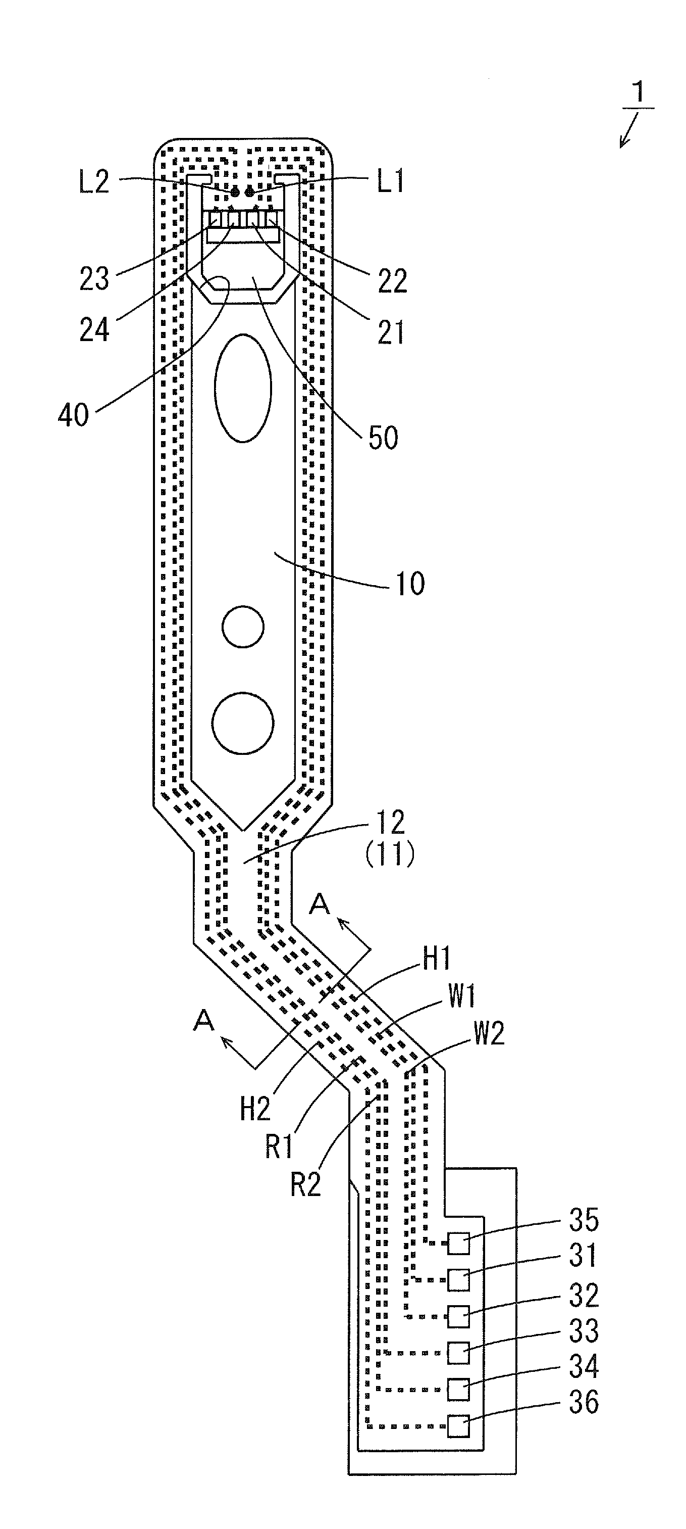
Plating apparatus, plating method, method of manufacturing printed circuit board and printed circuit board
- Summary
- Abstract
- Description
- Claims
- Application Information
AI Technical Summary
Benefits of technology
Problems solved by technology
Method used
Image

Examples
Example
(1-5-1) Inventive Example 1
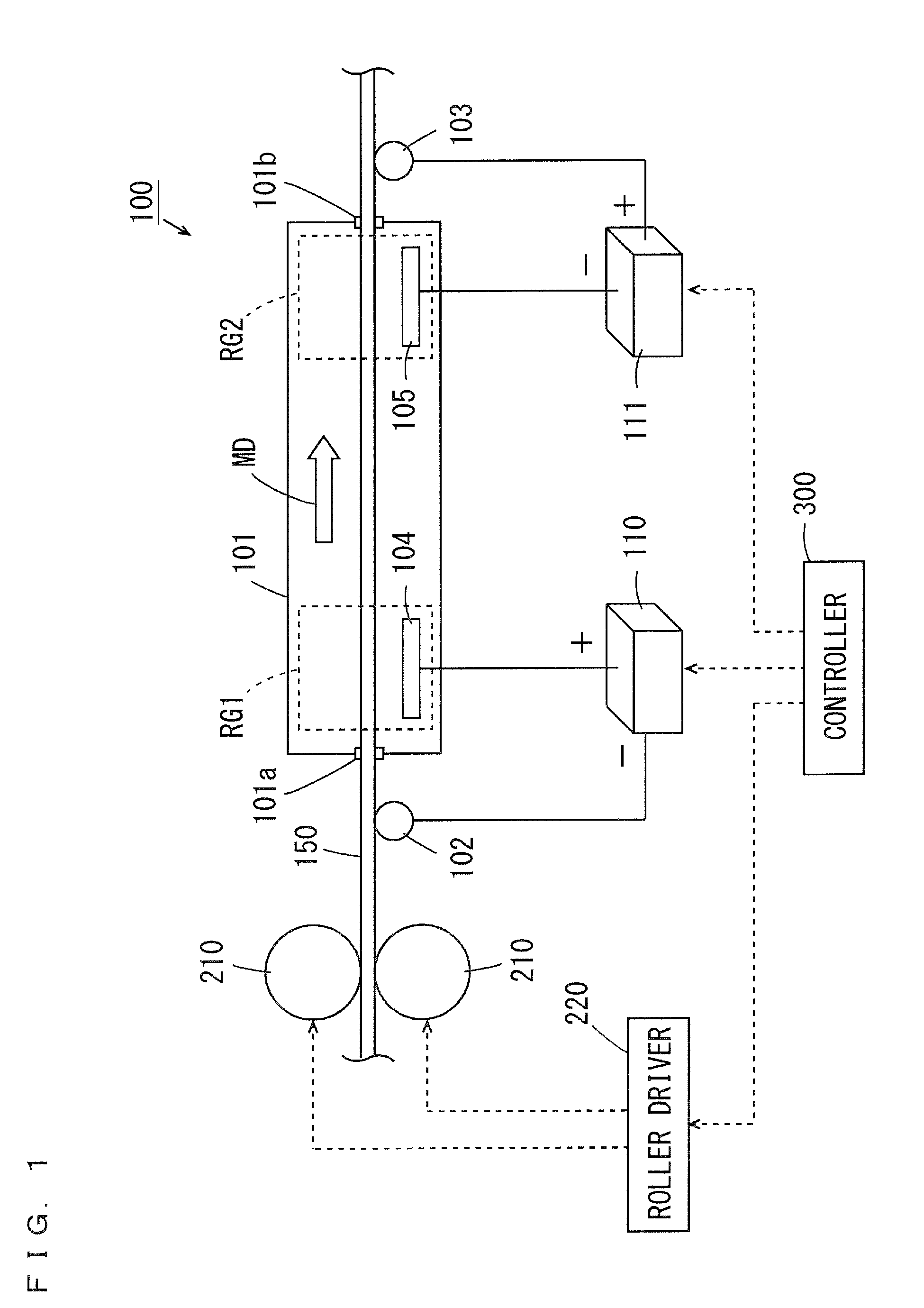
[0083]The stainless steel plate 150 that is made of SUS 304 and has a thickness of 18 μm was used as the member to be plated. A degreasing process of the surface of the stainless steel plate 150 was performed using a degreasing liquid for 2 minutes, and the stainless steel plate 150 after the degreasing process was sufficiently washed with water. Thereafter, in the plating apparatus 100 of FIG. 1, the reverse electrolytic process and the electrolytic plating process were sequentially performed on one portion to be plated.
[0084]An aqueous solution including nickel sulphate was used as the electrolytic solution. The pH of the electrolytic solution was set to 0, the concentration of the nickel sulphate in the electrolytic solution was set to 200 g / L and the concentration of sulfuric acid was set to 40 g / L. Further, the temperature of the electrolytic solution was set to 30° C. Further, the current density in the electrolytic solution applied by the rectifier ...
Example
(1-5-2) Inventive Example 2
[0085]The reverse electrolytic process and the electrolytic plating process were performed similarly to the above-mentioned inventive example 1 except that the pH of the electrolytic solution in the plating tank 101 was set to 1.0, and a time period for the electrolytic plating process was set to 1 minute.
Example
(1-5-3) Inventive Example 3
[0086]The reverse electrolytic process and the electrolytic plating process were performed similarly to the above-mentioned inventive example 1 except that the pH of the electrolytic solution in the plating tank 101 was set to 4.0, and a time period for the electrolytic plating process was set to 1 minute.
PUM
| Property | Measurement | Unit |
|---|---|---|
| Electric potential / voltage | aaaaa | aaaaa |
Abstract
Description
Claims
Application Information
 - Generate Ideas
- Intellectual Property
- Life Sciences
- Materials
- Tech Scout
- Unparalleled Data Quality
- Higher Quality Content
- 60% Fewer Hallucinations
Browse by: Latest US Patents, China's latest patents, Technical Efficacy Thesaurus, Application Domain, Technology Topic, Popular Technical Reports.
© 2025 PatSnap. All rights reserved.Legal|Privacy policy|Modern Slavery Act Transparency Statement|Sitemap|About US| Contact US: help@patsnap.com