Display panel
- Summary
- Abstract
- Description
- Claims
- Application Information
AI Technical Summary
Benefits of technology
Problems solved by technology
Method used
Image
Examples
Embodiment Construction
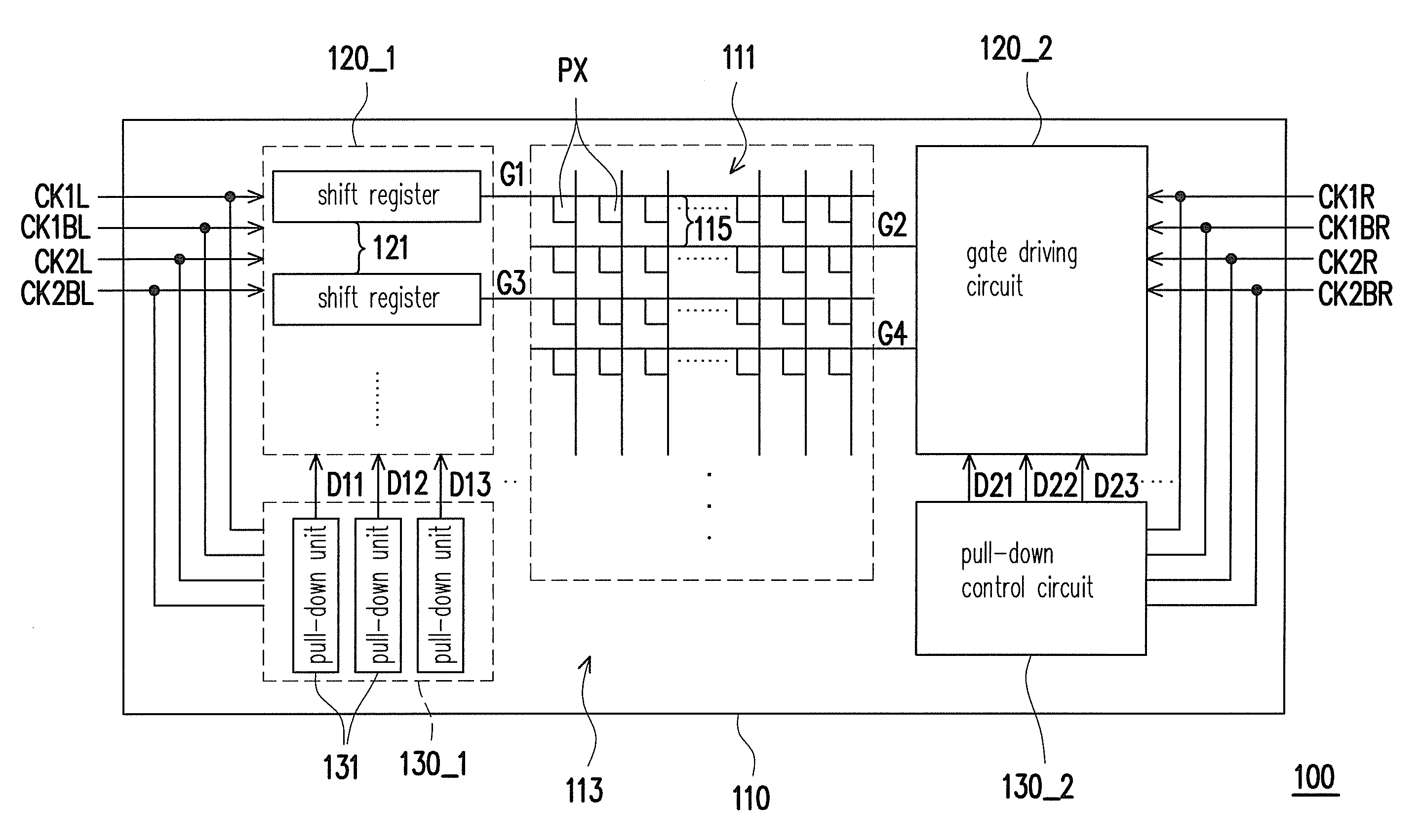
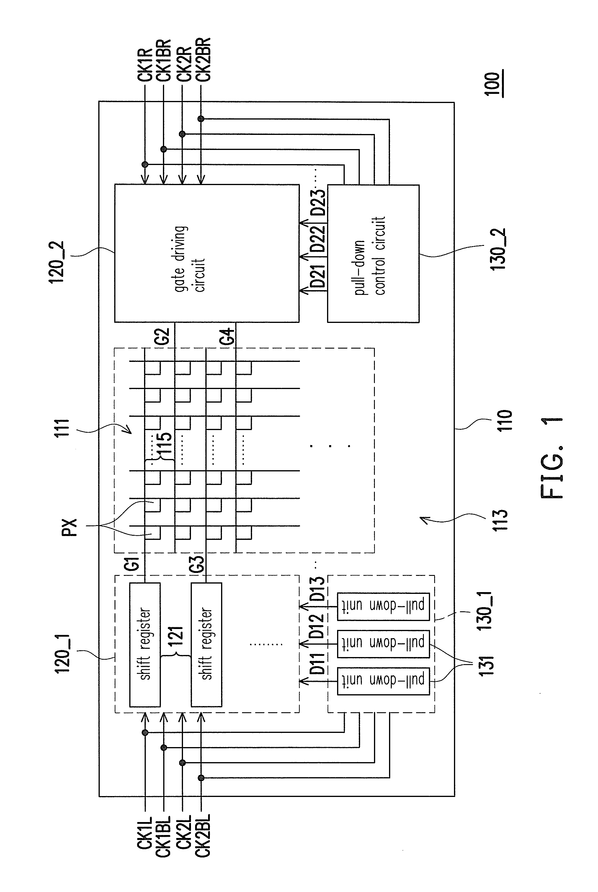
[0024]FIG. 1 is a schematic system diagram of a display panel according to an embodiment of the invention. The display panel 100 includes a substrate 110, a plurality of pixels PX, a plurality of scan lines 115, gate driving circuits 120_1 and 120_2, and pull-down control circuits 130_1 and 130_2. The substrate 100 has a display area 111 and a peripheral area 113. The pixels PX are disposed on the display area 111. The scan lines 115 are disposed on the substrate 111, are respectively coupled to the corresponding pixels PX, and extend from the display area 111 to the peripheral area 113, so that the scan lines 115 are coupled to the corresponding gate driving circuits (such as 120_1 and 120_2).
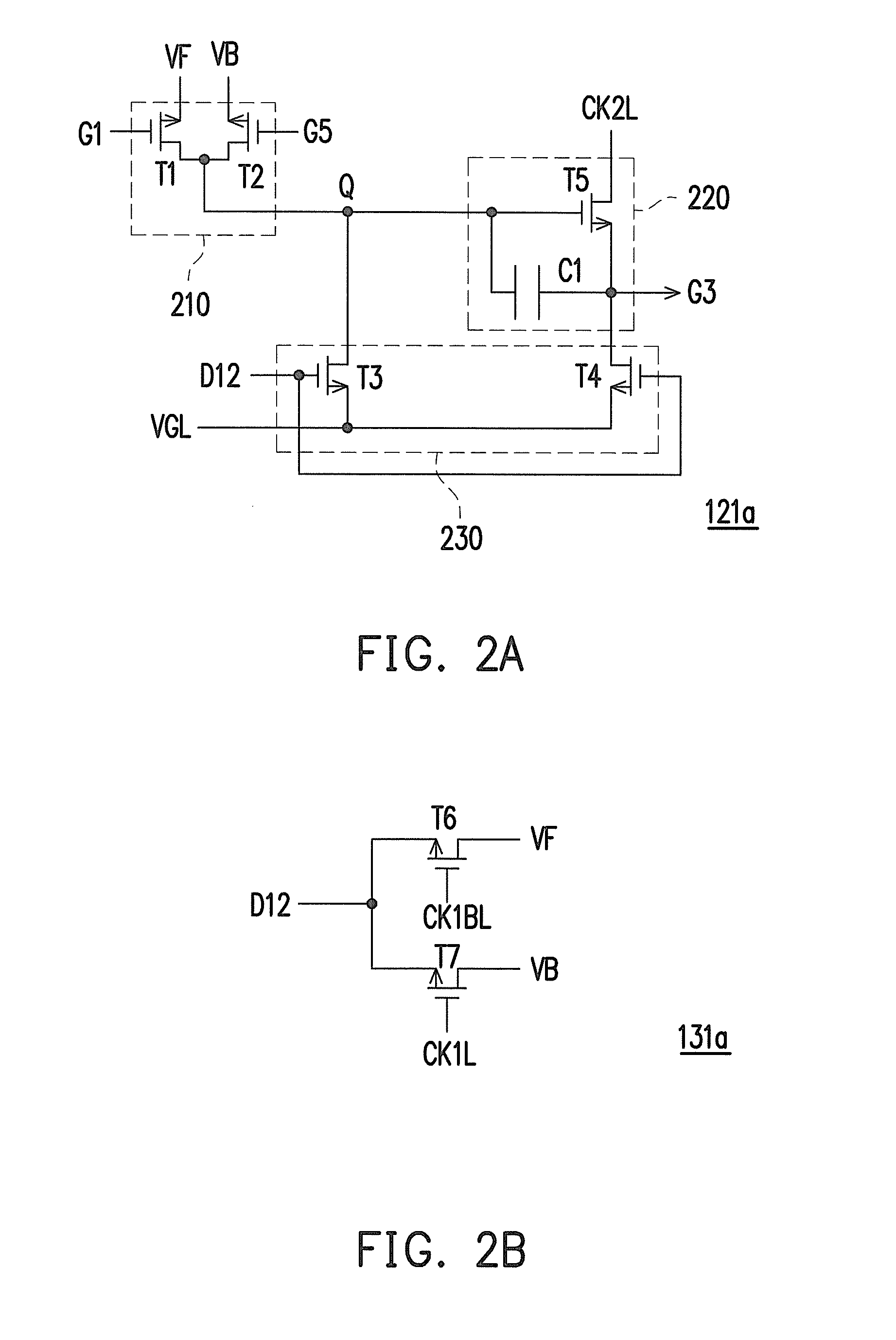
[0025]The pull-down control circuit 130_1 is disposed on the peripheral area 113, receives a plurality of clock signals (e.g., four clock signals CK1L, CK1BL, CK2L, and CK2BL), and has a plurality of pull-down units 131 to provide a plurality of the first pull-down signals (such as D11 to D13)...
PUM
 Abstract
Description
Claims
Application Information


