Systems and Methods for Lithography Masks

a technology of lithography mask and system, applied in the field of systems and methods for lithography mask, can solve the problems of reducing the accuracy of lithography mask,

Inactive Publication Date: 2014-11-13
TAIWAN SEMICON MFG CO LTD
View PDF0 Cites 0 Cited by
  • Summary
  • Abstract
  • Description
  • Claims
  • Application Information

AI Technical Summary

Problems solved by technology

If a mask is not able to precisely form a pattern in a photoresist, the subsequently formed feature may not meet its critical dimension requirement.
For advanced lithography imaging, the improvement of resolution is one tough challenge.
Conventiona

Method used


Image

  • Systems and Methods for Lithography Masks
  • Systems and Methods for Lithography Masks
  • Systems and Methods for Lithography Masks

Examples


Embodiment Construction

[0011]The making and using of the present embodiments are discussed in detail below. It should be appreciated, however, that the present disclosure provides many applicable inventive concepts that can be embodied in a wide variety of specific contexts. The specific embodiments discussed are merely illustrative of specific ways to make and use the disclosed subject matter, and do not limit the scope of the different embodiments.

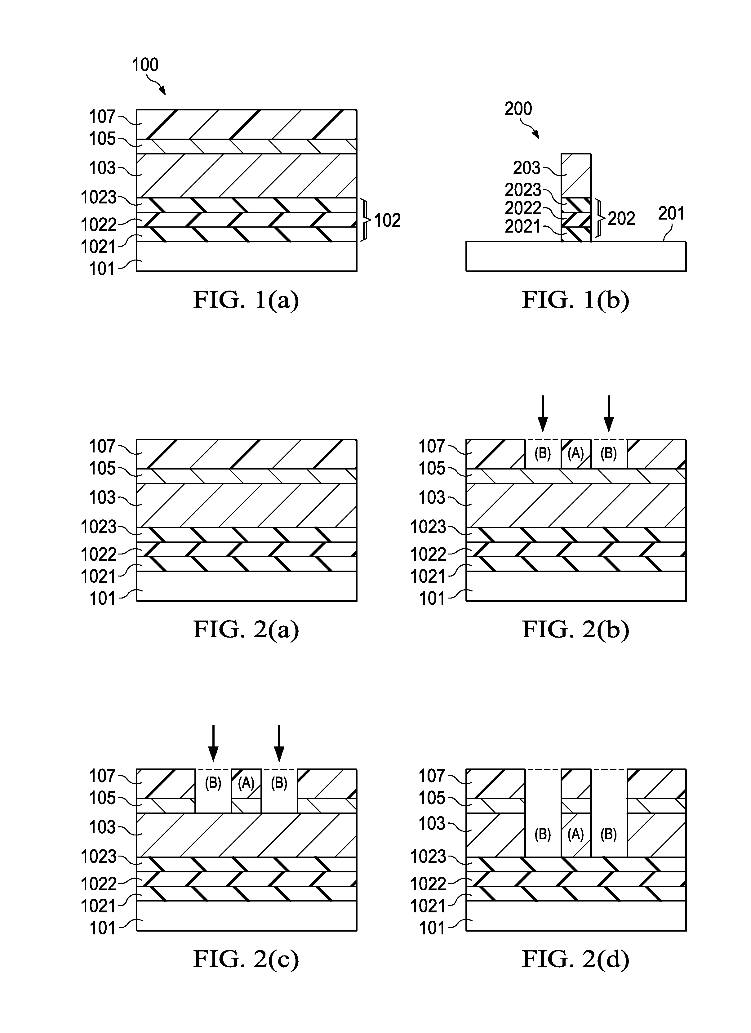
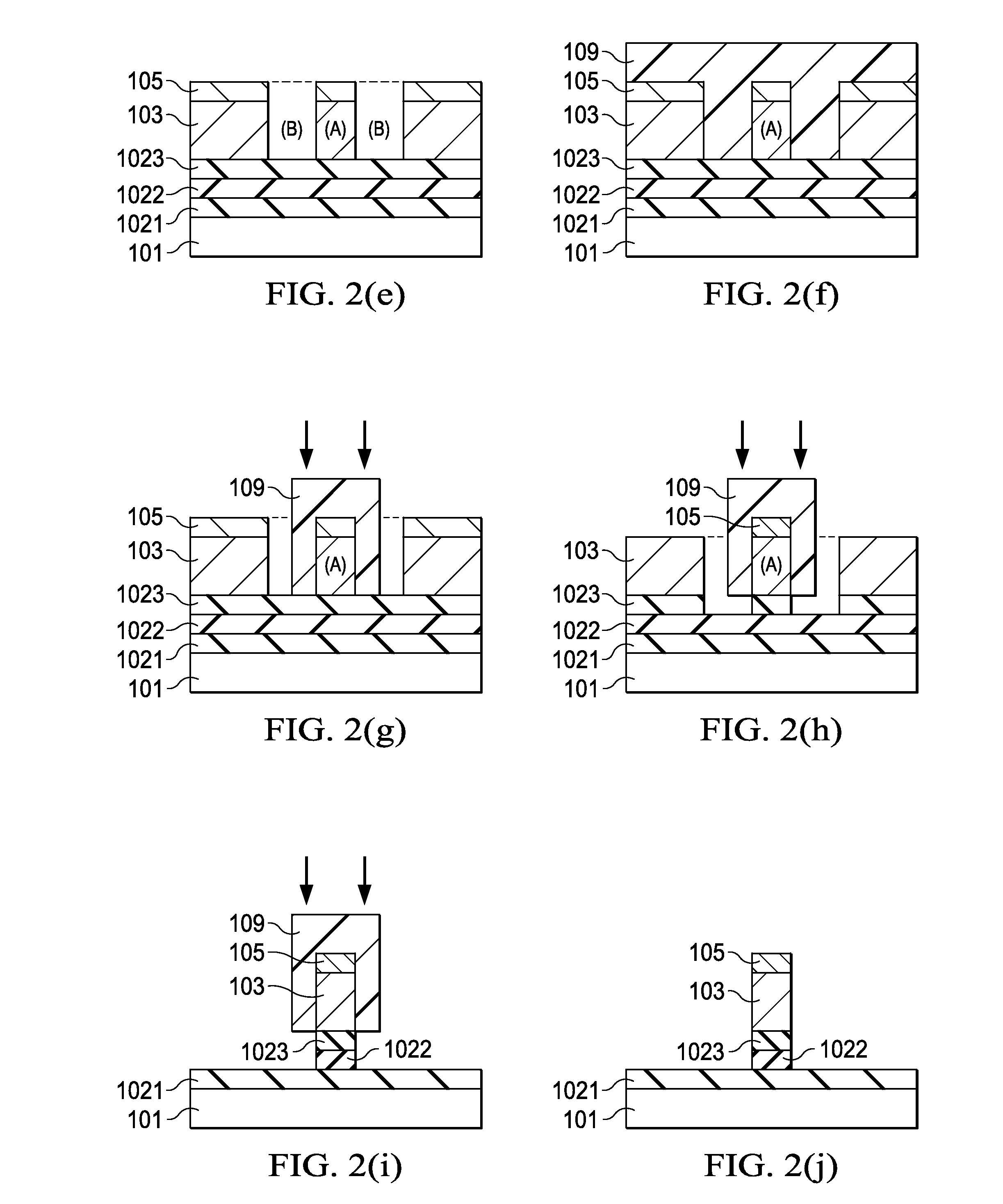
[0012]Embodiments will be described with respect to specific contexts, namely the structure of mask blanks and masks, and the methods of making masks. Through newly designed mask blank structures, new pattern sizing rules, and new process flows, lower quartz damage can be achieved for negative tone imaging (NTI) bright masks. The new mask blank and the new mask comprise a tripe etching stop layer which can prevent damages to the quartz substrate when the process goes through etching steps three times. The triple etching stop layer may comprise a first sub-laye...


PUM


Abstract

Structure of mask blanks and masks, and methods of making masks are disclosed. The new mask blank and mask comprise a tripe etching stop layer to prevent damages to the quartz substrate when the process goes through etching steps three times. The triple etching stop layer may comprise a first sub-layer of tantalum containing nitrogen (TaN), a second sub-layer of tantalum containing oxygen (TaO), and a third sub-layer of TaN. Alternatively, the triple etching stop layer may comprise a first sub-layer of SiON material, a second sub-layer of TaO material, and a third sub-layer of SiON material. Another alternative may be one layer of low etching rate MoxSiyONz material which can prevent damages to the quartz substrate when the process goes through etching steps three times. The island mask is defined on the mask blank by using various optical proximity correction rules.

Description

RELATED CASES[0001]This application is a divisional of U.S. patent application Ser. No. 13 / 486,015, filed on Jun. 1, 2012, and entitled, “Systems and Methods for Lithography Masks,” which application is incorporated herein by reference.BACKGROUND[0002]In semiconductor processing, multiple lithography steps are generally used to form a semiconductor chip. These steps typically include forming a photoresist over a substrate, exposing the photoresist to a pattern of light generally controlled by a mask, developing the pattern in the photoresist to expose the underlying substrate, and etching the pattern in the underlying substrate. The pattern etched in the underlying substrate may be a basis for some feature formation, such as an ion impurity implantation such as for doping source and drain regions, a formation of a structure like a gate pattern, or a pattern for a conductive material such as in a metallization layer.[0003]Photoresists may be classified into two groups: positive resis...

Claims


Application Information

Patent Timeline
IPC IPC(8): G03F1/36
CPCG03F1/36G03F1/50G03F1/58G03F1/80
Inventor TU, CHIH-CHIANGLEE, HSIN-CHANGCHANG, JONG-YUHCHEN, CHIA-JENCHEN, CHUN-LANG
Owner TAIWAN SEMICON MFG CO LTD
Why Eureka
Try Eureka