
TFT with insert in passivation layer or etch stop layer

Inactive Publication Date: 2014-11-20
APPLIED MATERIALS INC
View PDF6 Cites 4 Cited by
  • Summary
  • Abstract
  • Description
  • Claims
  • Application Information

AI Technical Summary

Benefits of technology

The present invention relates to controlling the threshold voltage and off-current of a thin film transistor. The patent describes semiconductor devices with a thin film transistor including a substrate, first and second passivation layers, a slot or trench, and a silicon nitride layer. The method also describes depositing a first and second passivation layers and a silicon oxide layer within a trench. The technical effects include controlling the threshold voltage and off-current of the thin film transistor and improving the stability and reliability of the semiconductor device.

Problems solved by technology

Current MO-TFTs, such as indium gallium zinc oxide (IGZO), zinc oxide (ZnO) and zinc oxynitride (ZnON) TFT devices, have interface problems which can include mobility problems and offset turn on voltages.

Method used


Image

  • TFT with insert in passivation layer or etch stop layer
  • TFT with insert in passivation layer or etch stop layer
  • TFT with insert in passivation layer or etch stop layer

Examples


Embodiment Construction

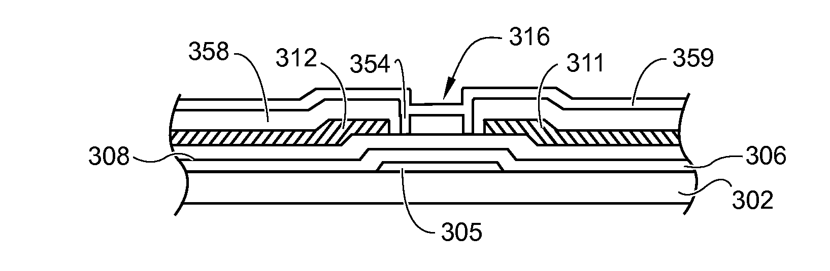
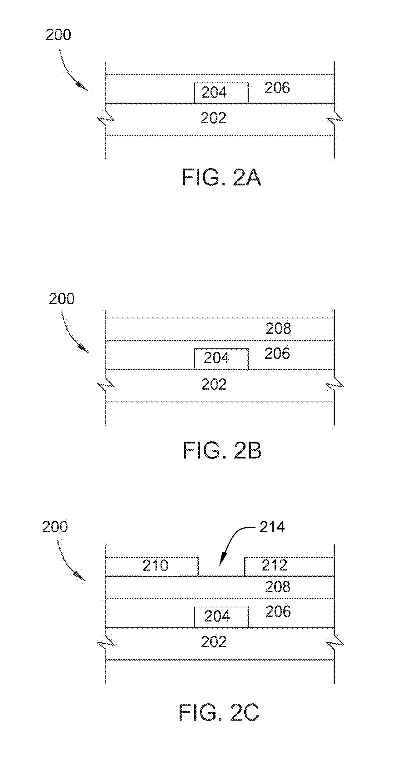
[0016]The present invention generally relates to using trenches in the passivation layer to control the threshold voltage of a TFT. A TFT has a threshold voltage which is the voltage at the gate which is required for current to flow between the source and the drain. By forming one or more slots or trenches through the passivation layer, and then filling the slots or trenches with additional passivation material, the threshold voltage can be corrected such that current flow is better controlled by the gate when the gate is either on or off based on voltage received.

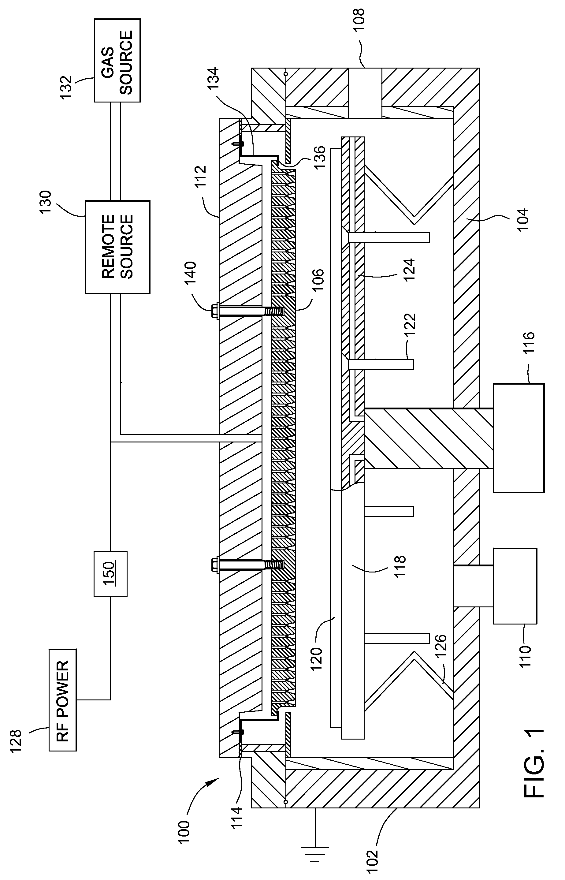
[0017]The invention is illustratively described below utilized in a processing system, such as a plasma enhanced chemical vapor deposition (PECVD) system available from AKT America, a division of Applied Materials, Inc., located in Santa Clara, Calif. However, it should be understood that the invention has utility in other system configurations, including those sold by other manufacturers.

[0018]FIG. 1 is a schematic, cross...


PUM


Abstract

Embodiments disclosed herein generally relate to thin film transistors with one or more trenches to control the threshold voltage and off-current and methods of making the same. In one embodiment, a semiconductor device can include a substrate comprising a surface with a thin film transistor formed thereon, a first passivation layer formed over the thin film transistor, a trench formed within the first passivation layer and a second passivation layer formed over the first passivation layer and within the trench.

Description

CROSS-REFERENCE TO RELATED APPLICATIONS[0001]This application claims benefit of U.S. Provisional Patent Application Ser. No. 61 / 823,336, filed May 14, 2013 (APPM / 17011USL), which is incorporated herein by reference.BACKGROUND OF THE INVENTION[0002]1. Field of the Invention[0003]Embodiments of the present invention generally relate to improving the threshold voltage in a thin film transistor (TFT).[0004]2. Description of the Related Art[0005]Current interest in TFT arrays is particularly high because these devices may be used in liquid crystal active matrix displays (LCDs) of the kind often employed for computer and television flat panels. The LCDs may also contain light emitting diodes (LEDs), such as organic light emitting diodes (OLEDs) for back lighting. The LEDs and OLEDs require TFTs for addressing the activity of the displays.[0006]The current driven through the TFTs (i.e., the on-current) is limited by the channel material (often referred to as the active material, semiconduc...

Claims


Application Information

Patent Timeline
IPC IPC(8): H01L29/786H01L29/24H01L21/283
CPCH01L29/7869H01L29/24H01L21/283
Inventor YE, YANYOU, HARVEY
Owner APPLIED MATERIALS INC
Features
  • Generate Ideas
  • Intellectual Property
  • Life Sciences
  • Materials
  • Tech Scout
  • Unparalleled Data Quality
  • Higher Quality Content
  • 60% Fewer Hallucinations
Learn More