Semiconductor device
a technology of semiconductors and transistors, applied in the direction of semiconductor devices, electrical equipment, transistors, etc., can solve the problems of reducing reliability and electrical characteristics, and achieve the effect of reducing the variation in the electrical characteristics of transistors, reducing the formation of trap states, and reducing the deterioration of transistor electrical characteristics
- Summary
- Abstract
- Description
- Claims
- Application Information
AI Technical Summary
Benefits of technology
Problems solved by technology
Method used
Image

Examples
embodiment 1
[0074]In this embodiment, one embodiment of a semiconductor device and a method for manufacturing the semiconductor device will be described with reference to FIGS. 1A to 1C, FIGS. 2A to 2C, FIGS. 3A to 3C, and FIGS. 4A to 4C. In this embodiment, a transistor including an oxide semiconductor is shown as an example of the semiconductor device.
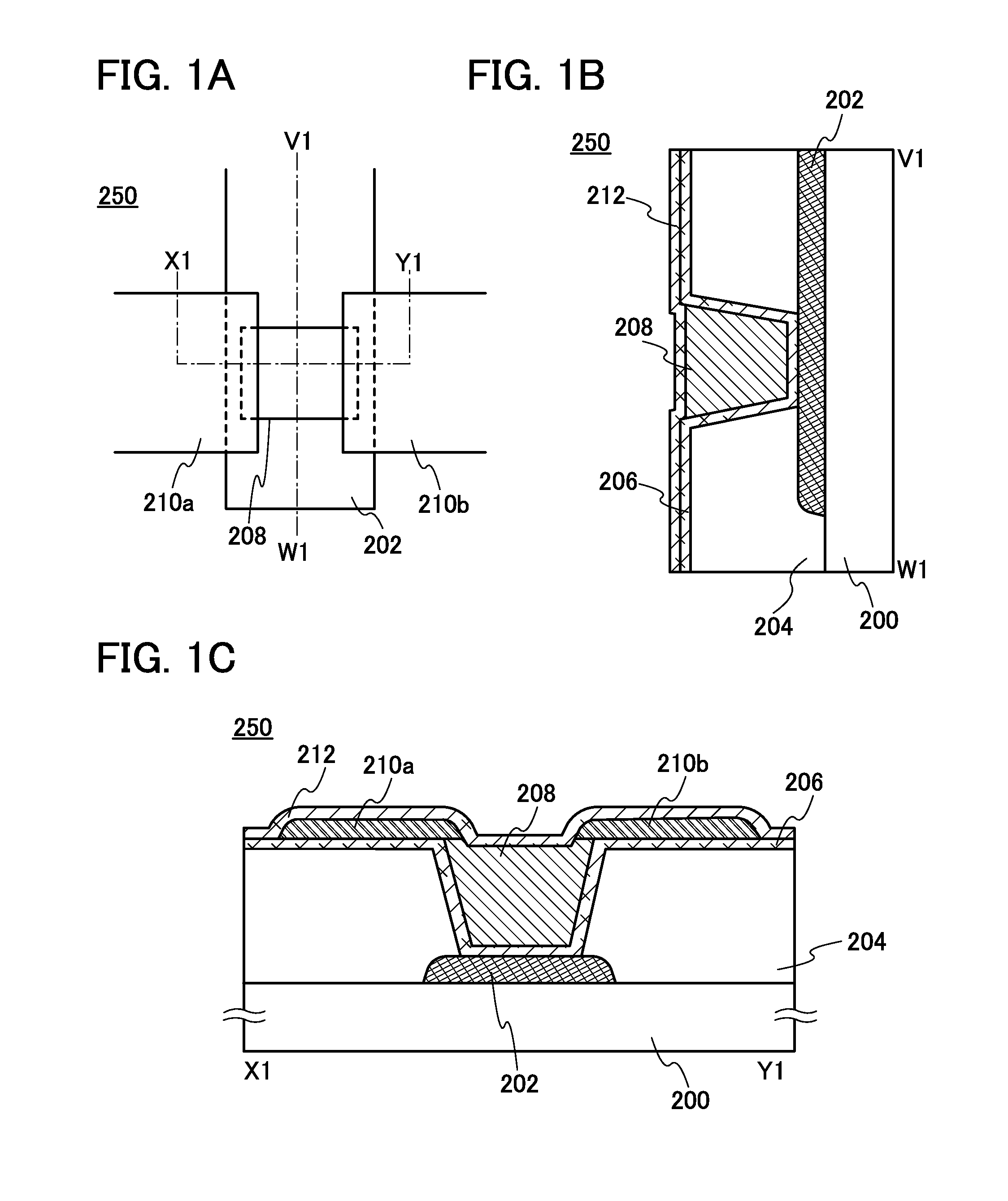
[0075]FIGS. 1A to 1C illustrate an example of a structure of a transistor 250. FIG. 1A is a plan view of the transistor 250, FIG. 1B is a cross-sectional view taken along line V1-W1 in FIG. 1A, and FIG. 1C is a cross-sectional view taken along line X1-Y1 in FIG. 1A. Note that in FIG. 1A, some components of the transistor 250 (e.g., an insulating layer 212) are not illustrated to avoid complexity. The same applies to the other plan views in this specification.
[0076]The transistor 250 illustrated in FIGS. 1A to 1C includes a gate electrode layer 202 over a substrate 200; an insulating layer 204 having an island-like groove; an insulating layer 206...
embodiment 2
[0145]In this embodiment, a structure of the semiconductor device different from that in Embodiment 1 will be described with reference to FIGS. 5A to 5D. For the components similar to those in Embodiment 1, the description of Embodiment 1 can be referred to and is not repeated in some cases.
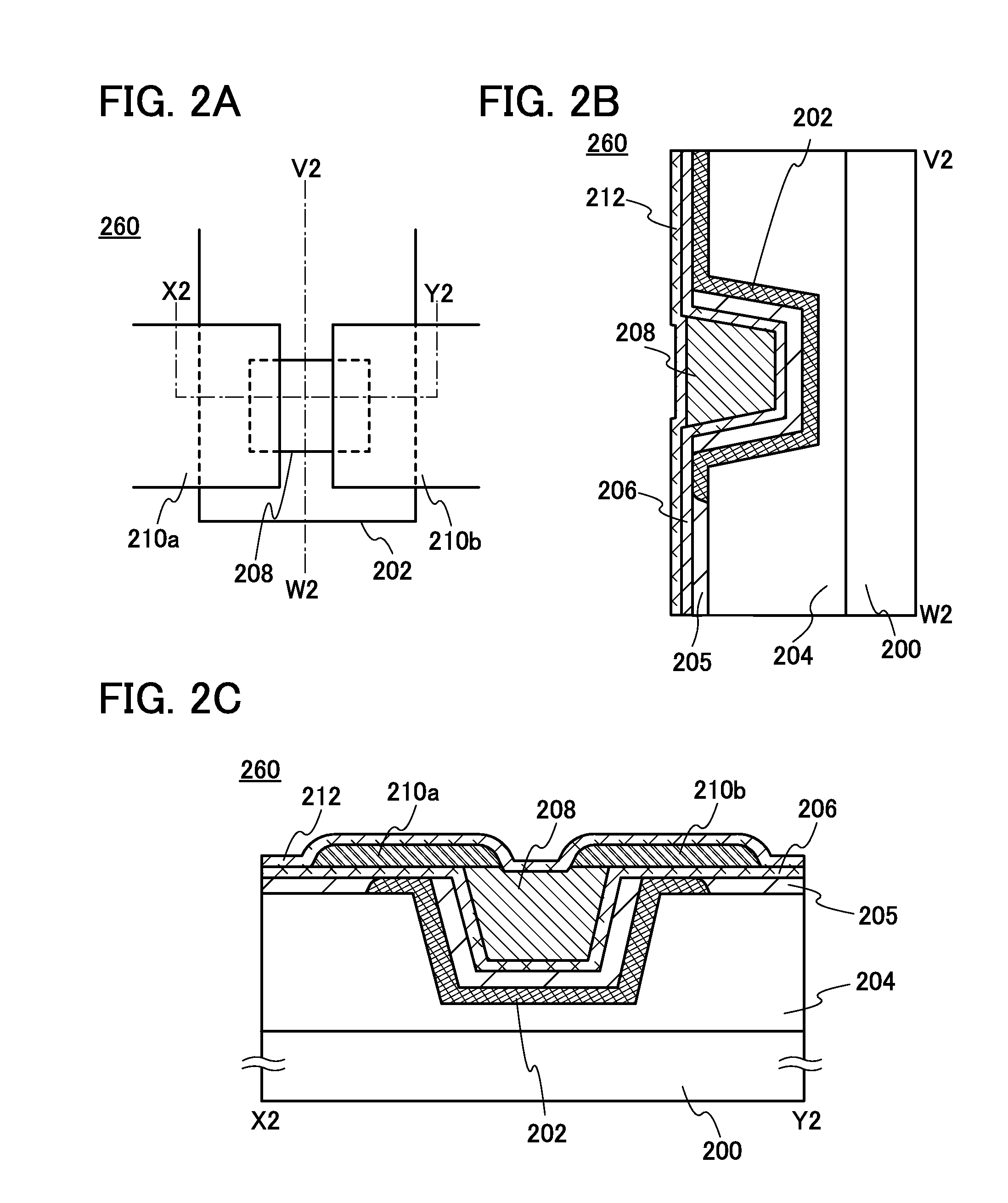
[0146]FIGS. 5A to 5D illustrate an example of a structure of a transistor 280. FIG. 5A is a plan view of the transistor 280, FIG. 5B is a cross-sectional view taken along line V3-W3 in FIG. 5A, and FIG. 5C is a cross-sectional view taken along line X3-Y3 in FIG. 5A. FIG. 5D is a band diagram schematically showing the energy at the bottom of the conduction band of a layered structure included in the transistor 280.
[0147]The transistor 280 illustrated in FIGS. 5A to 5C includes, like the transistor 260 in Embodiment 1, the insulating layer 204 which is over the substrate 200 and has an island-like groove; the gate electrode layer 202 in contact with a side surface and a bottom surface of the groove...
embodiment 3
[0184]In this embodiment, structures of the semiconductor device different from those in Embodiments 1 and 2, and an embodiment of a method for manufacturing the semiconductor device will be described with reference to FIGS. 6A to 6C, FIGS. 7A to 7C, FIGS. 8A to 8D, and FIGS. 9A to 9C.
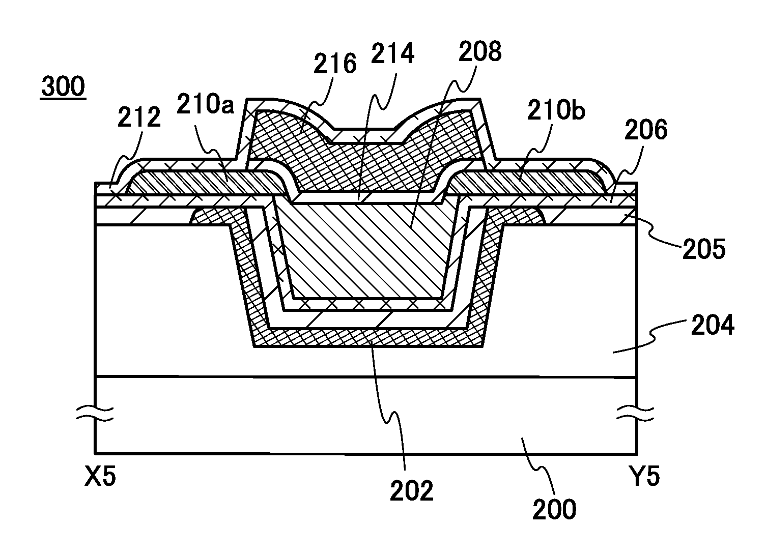
[0185]FIGS. 6A to 6C illustrate an example of a structure of a transistor 290. FIG. 6A is a plan view of the transistor 290, FIG. 6B is a cross-sectional view taken along line V4-W4 in FIG. 6A, and FIG. 6C is a cross-sectional view taken along line X4-Y4 in FIG. 6A. Note that in FIG. 6A, some components of the transistor 290 (e.g., the insulating layer 212) are not illustrated to avoid complexity. The structure of the transistor 290 is similar to that of the transistor 250, except for the components described below.
[0186]The transistor 290 illustrated in FIGS. 6A to 6C includes a first gate electrode layer 202 over the substrate 200; the insulating layer 204 having an island-like groove; the insulating...
PUM
 Abstract
Description
Claims
Application Information
 - R&D Engineer
- R&D Manager
- IP Professional
- Industry Leading Data Capabilities
- Powerful AI technology
- Patent DNA Extraction
Browse by: Latest US Patents, China's latest patents, Technical Efficacy Thesaurus, Application Domain, Technology Topic.
© 2024 PatSnap. All rights reserved.Legal|Privacy policy|Modern Slavery Act Transparency Statement|Sitemap