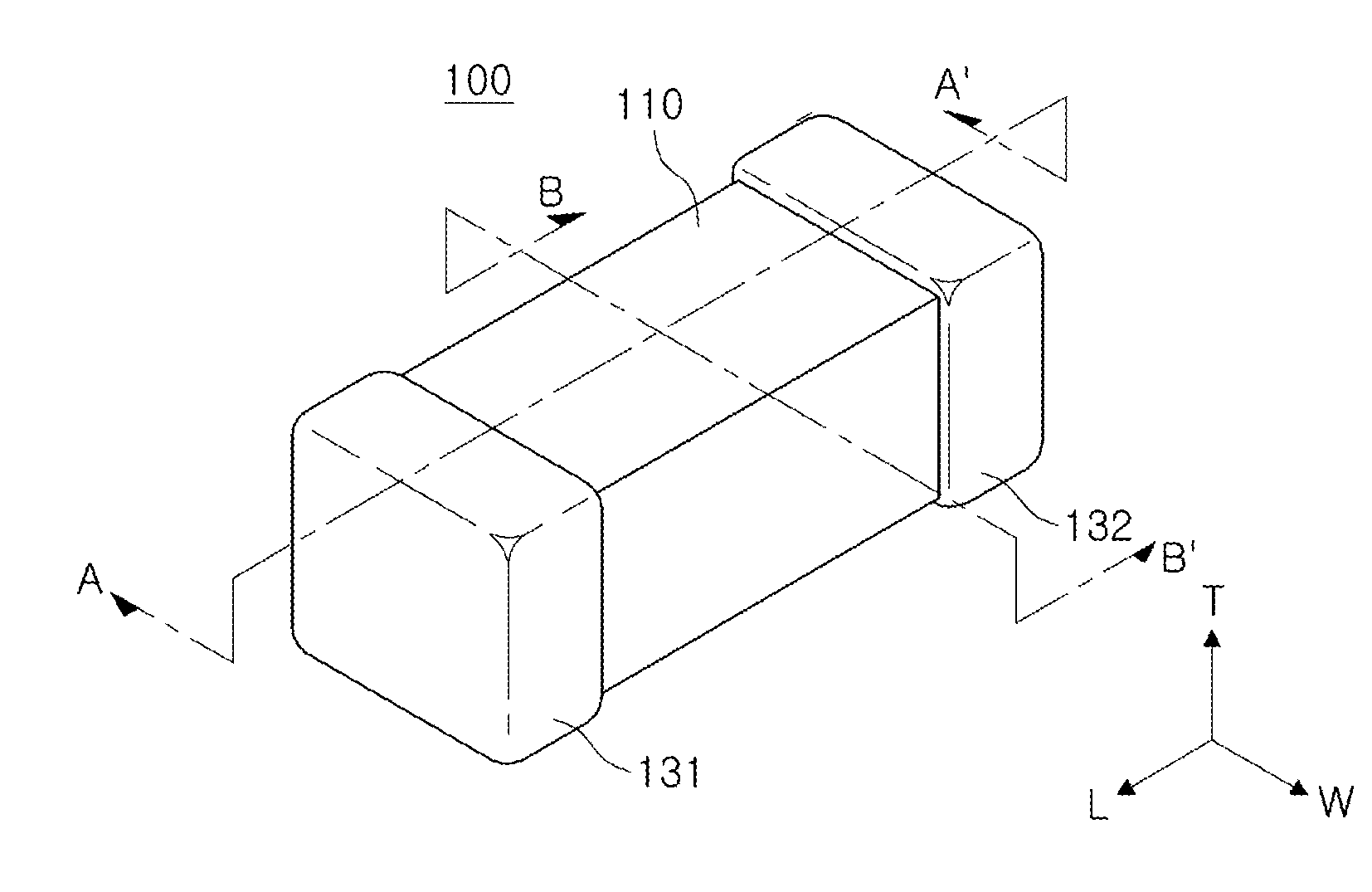
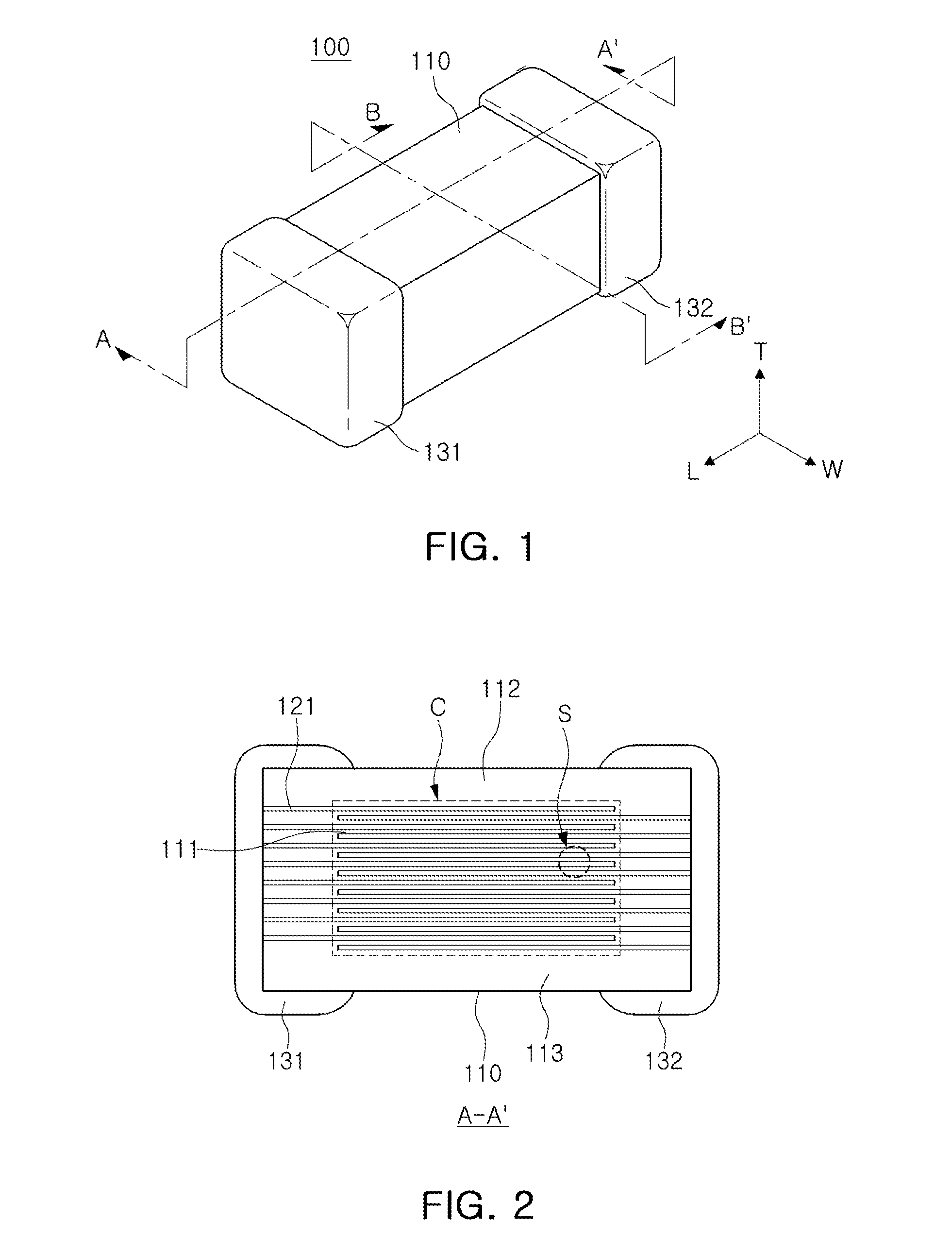
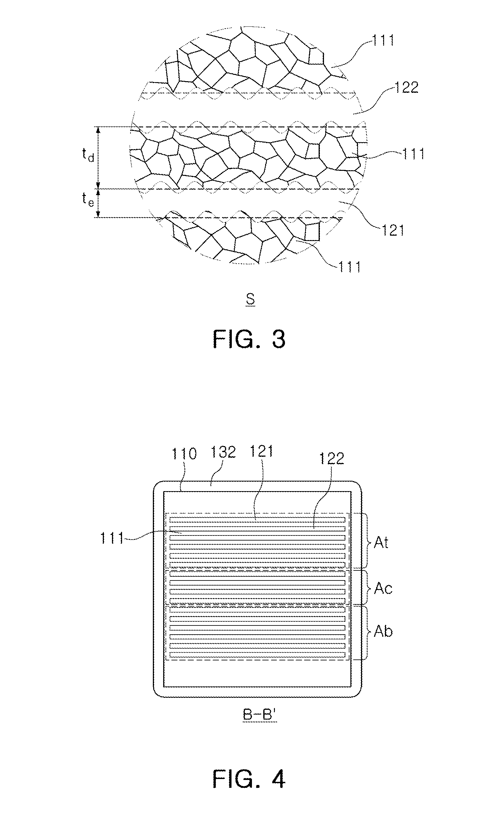
Multilayer ceramic electronic component and method of manufacturing the same
a technology of ceramic electronic components and ceramic ceramics, applied in the direction of fixed capacitor details, stacked capacitors, fixed capacitors, etc., can solve the problem of not revealing the numerical definition of limiting the connectivity of internal electrodes, and achieve the effects of preventing internal cracks during firing, high capacitance, and improved reliability
- Summary
- Abstract
- Description
- Claims
- Application Information
AI Technical Summary
Benefits of technology
Problems solved by technology
Method used
Image

Examples
experimental example
[0094]Multilayer ceramic capacitors according to embodiments of the present invention and comparative examples are manufactured using the following method, but the embodiments of the present invention are not limited thereto.
[0095]Here, a conductive paste for an internal electrode was prepared using a nickel metal powder having average particle size distribution (D50) of 80 to 120 nm, and the content of nickel metal powder is 45 to 55% based on a total amount.
[0096]The conductive paste for the internal electrode was printed on the green sheet including a ceramic powder particle having an average particle size distribution (D50) of 80 to 120 nm using a screen printing method to form the internal electrode, and 200 to 270 layers of green sheets were stacked to prepare a multilayer structure.
[0097]Then, the multilayer structure was compressed and cut to prepare a 1005-sized chip, and the chip was fired under a reduction atmosphere equal to or less than H2 of 0.1% at a temperature of 10...
PUM
| Property | Measurement | Unit |
|---|---|---|
| particle size distribution | aaaaa | aaaaa |
| thickness | aaaaa | aaaaa |
| thickness | aaaaa | aaaaa |
Abstract
Description
Claims
Application Information