Optical Sensor
a technology of optical sensors and optical slits, applied in the field of optical sensors, can solve the problems of false detection of movement directions, inability to accurately obtain phase differences between reflected light and movement direction, etc., and achieve the effects of improving detection resolution, reducing light emission angles, and improving s/n
- Summary
- Abstract
- Description
- Claims
- Application Information
AI Technical Summary
Benefits of technology
Problems solved by technology
Method used
Image

Examples
first embodiment
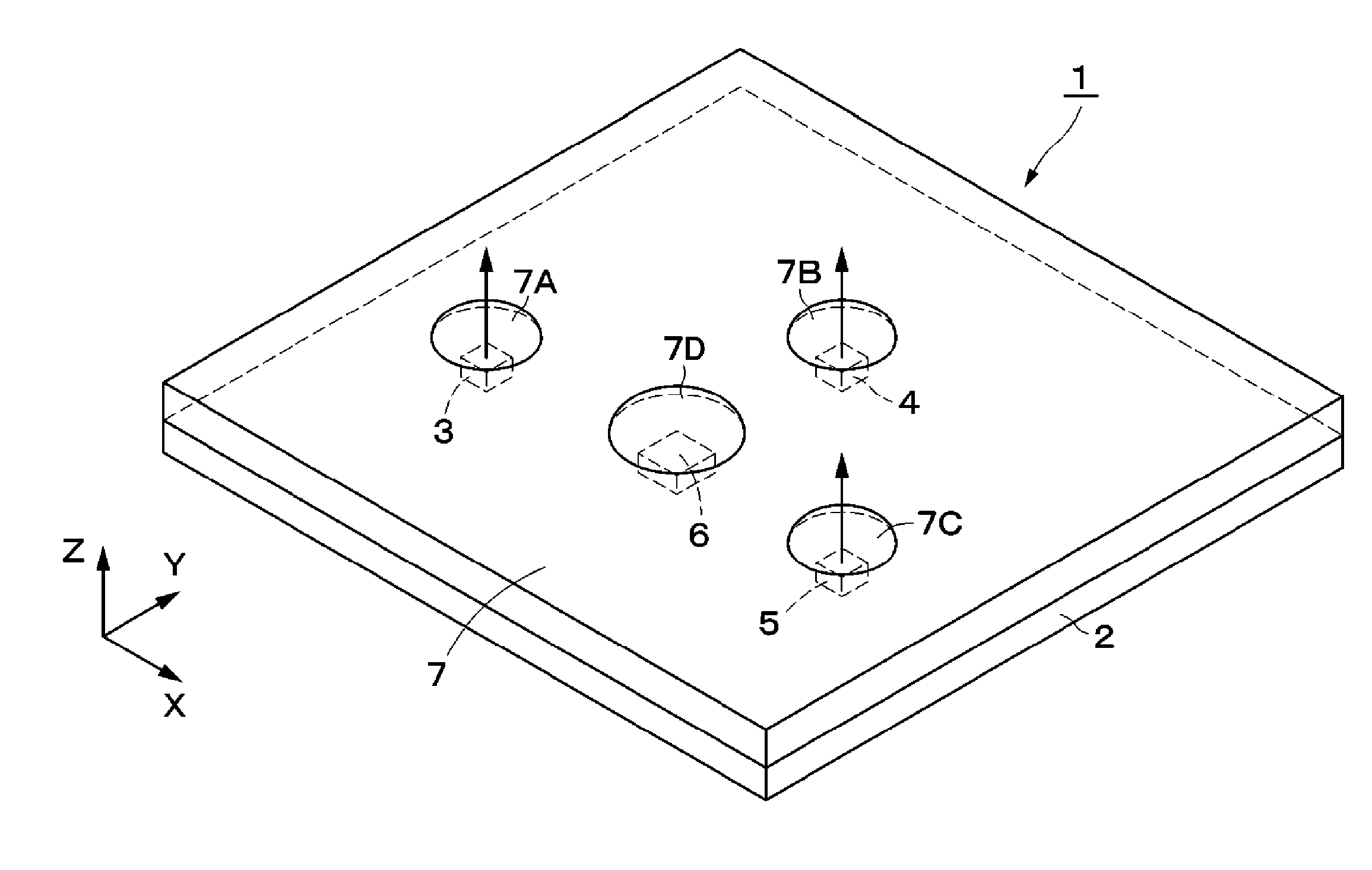
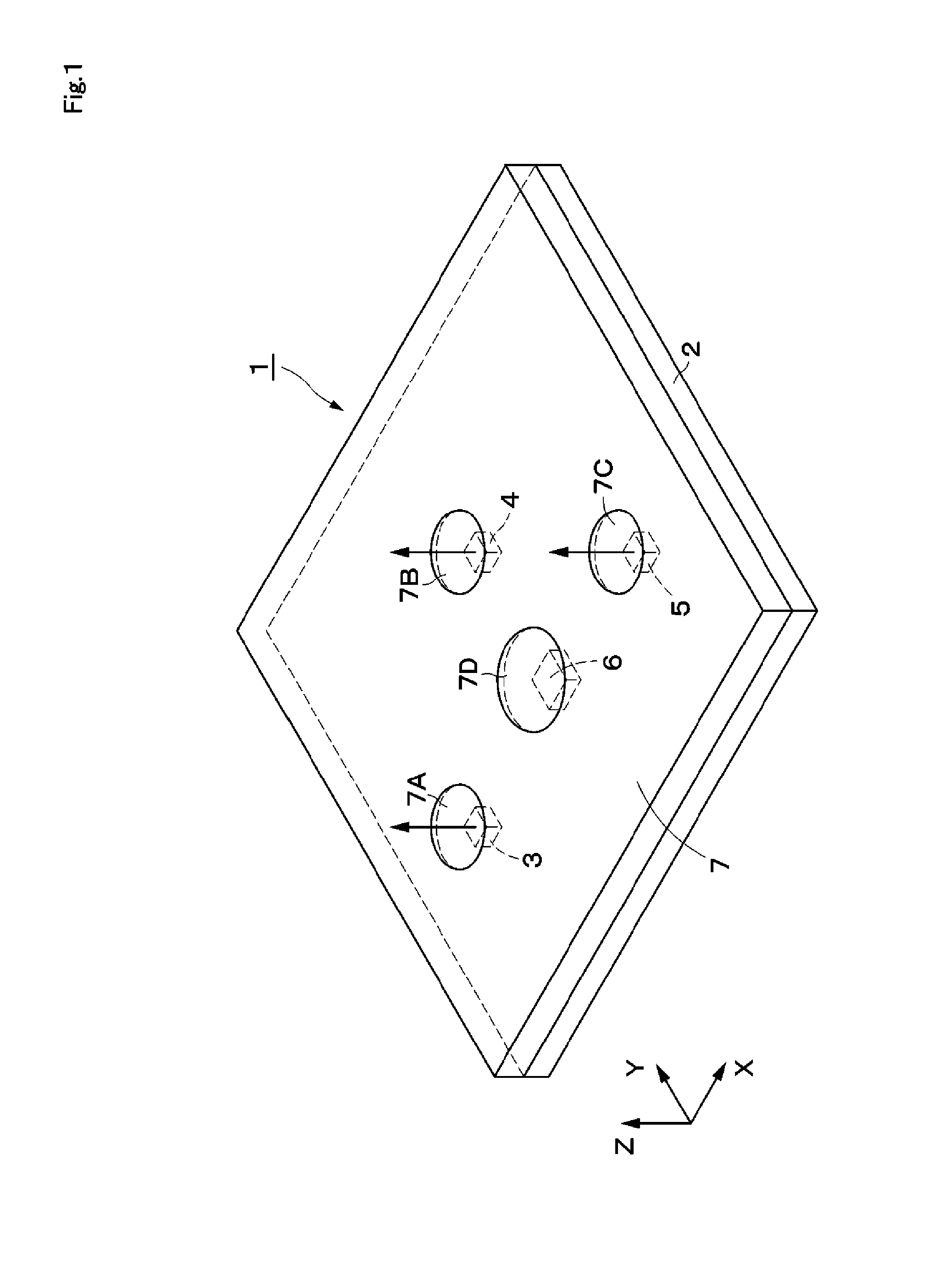
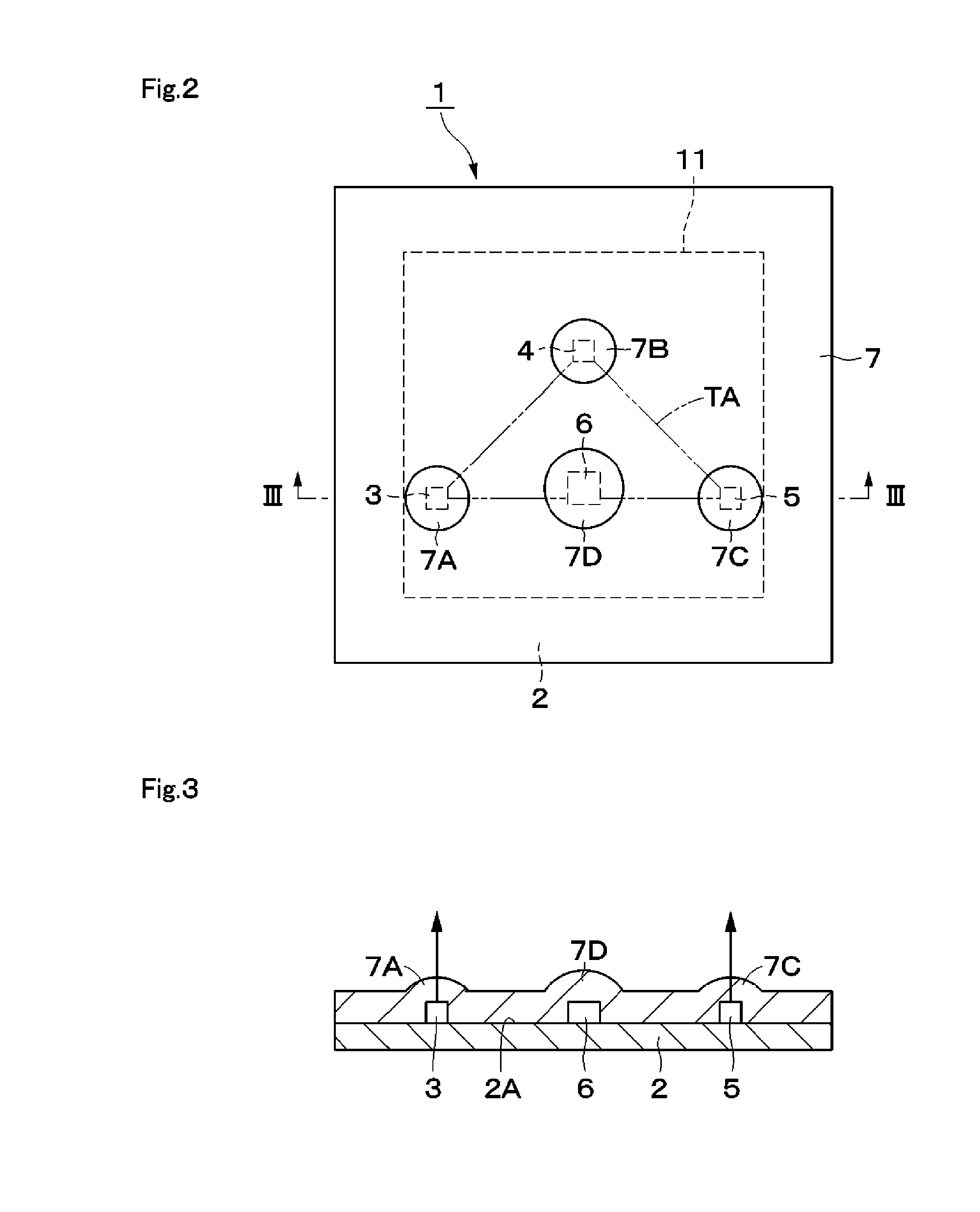
[0050]FIGS. 1 to 4 show an optical sensor 1 according to a The optical sensor 1 includes a substrate 2, light emitting elements 3 to 5, a light receiving element 6, a signal processing circuit 11, and the like.
[0051]The substrate 2 is a flat plate formed from an insulating material. For example, a printed wiring board is used as the substrate 2. The light emitting elements 3 to 5 and the light receiving element 6 are mounted on a surface 2A of the substrate 2.
[0052]The light emitting elements 3 to 5 are mounted on the surface 2A of the substrate 2 and emit light such as infrared light or visible light. The optical axes of the light emitting elements 3 to 5 generally extend, for example, in a direction perpendicular to the surface 2A of the substrate 2 (in a Z-axis direction). For example, light emitting diodes (LEDs), laser diodes (LDs), or vertical cavity surface emitting lasers (VCSELs) are used as the light emitting elements 3 to 5. In order to increase detection resolution and ...
second embodiment
[0109]Next, a process of calculating the phase difference T21 will be described with reference to FIG. 28.
[0110]In step 41, a start time t0 and an end time t1 of the waveform are determined as a range for calculating the correlation between the waveforms, on the basis of the reflected light signals Sr1 and Sr2. In step 42, the maximum value (±x0) by which the waveform of the reflected light signal Sr2 is to be shifted to the negative side or the positive side is determined as a detection range of the phase difference T21 on the basis of the reflected light signals Sr1 and Sr2.
[0111]In step 43, a shift amount x is set at a negative maximum value (−x0) as an initial value. In step 44, the reflected light signal Sr2 is temporally shifted by the shift amount x using a function Zc1(x) shown in the following mathematical formula 5, and a product sum of the reflected light signals Sr1 and Sr2 is calculated in this state. In this case, the function Zc1(x) is a correlation function of the r...
third embodiment
[0119]In an optical sensor 31 three light receiving elements 32 to 34 are mounted on the substrate 2. The light receiving element 32 is located near the light emitting element 3 and receives the reflected light based on the light from the light emitting element 3. The light receiving element 33 is located near the light emitting element 4 and receives the reflected light based on the light from the light emitting element 4. The light receiving element 34 is located near the light emitting element 5 and receives the reflected light based on the light from the light emitting element 5.
[0120]In this case, the light emitting elements 3 to 5 do not need to emit light by pulse emission in a time-division manner, and may continuously emit light.
[0121]Thus, in the third embodiment as well, it is possible to obtain substantially the same advantageous effects as those in the first embodiment. In this case, light detection signals outputted from the three light receiving elements 32 to 34 cor...
PUM
 Abstract
Description
Claims
Application Information
 - R&D Engineer
- R&D Manager
- IP Professional
- Industry Leading Data Capabilities
- Powerful AI technology
- Patent DNA Extraction
Browse by: Latest US Patents, China's latest patents, Technical Efficacy Thesaurus, Application Domain, Technology Topic.
© 2024 PatSnap. All rights reserved.Legal|Privacy policy|Modern Slavery Act Transparency Statement|Sitemap