

Display device and electronic apparatus
- Summary
- Abstract
- Description
- Claims
- Application Information
AI Technical Summary
Benefits of technology
Problems solved by technology
Method used
Image

Examples
Embodiment Construction
[0031]Hereinafter, embodiments of the invention are described in detail with reference to the drawings. It should be noted that the same components are denoted by the same reference numerals, and the description thereof is omitted.
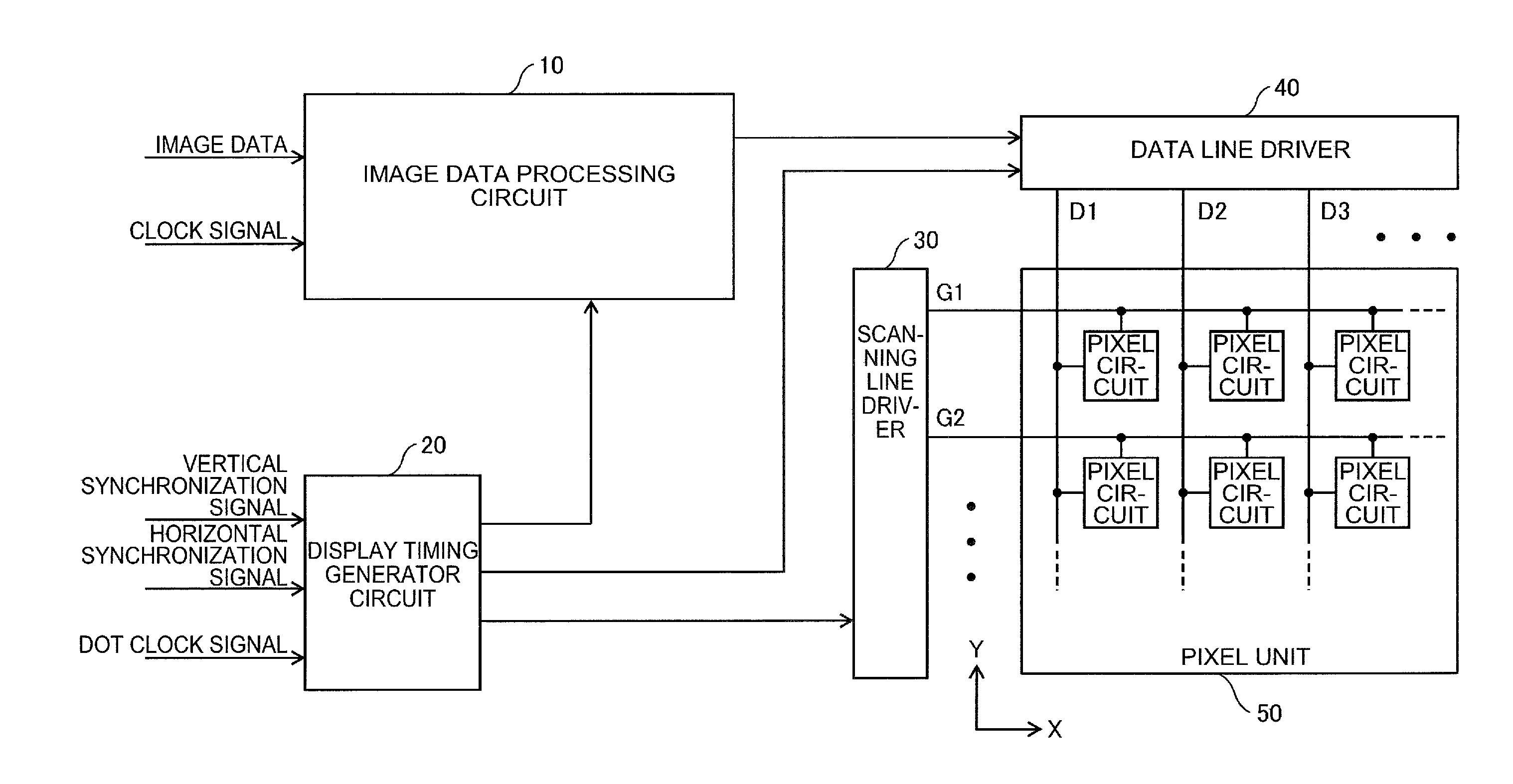
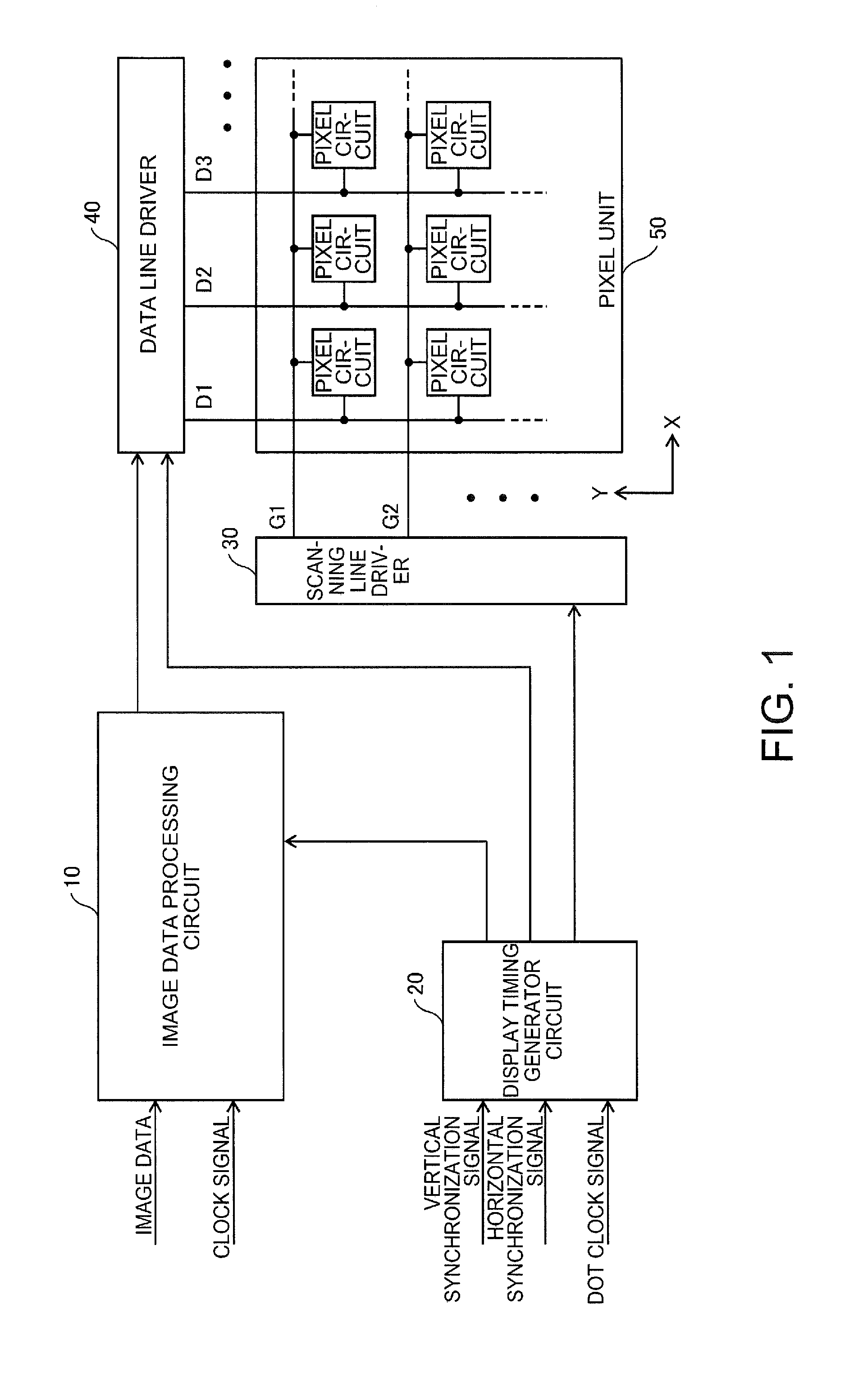
[0032]FIG. 1 is a block diagram showing a configuration of an electronic apparatus using a display device according to an embodiment of the invention. This electronic apparatus is an electronic apparatus such as an electronic viewfinder and a head mounted display. FIG. 1 shows only portions associated with image display.
[0033]As shown in FIG. 1, the electronic apparatus includes an image data processing circuit 10, a display timing generator circuit 20, a scanning line driver 30, a data line driver 40, and a pixel unit 50. Here, an active matrix display device using an organic EL panel is constituted by components including at least the scanning line driver 30 to the pixel unit 50.
[0034]The pixel unit 50 includes a plurality of pixel circuits formed respec...
PUM
 Abstract
Description
Claims
Application Information