Printed circuit board and manufacturing method thereof

a printed circuit board and manufacturing method technology, applied in the field can solve the problems of increasing the demand for high-density and miniaturized circuits, limiting the improvement of impedance performance, and complicated design so as to simplify the manufacturing process of printed circuit boards, increase productivity and product properties

Inactive Publication Date: 2015-01-15
SAMSUNG ELECTRO MECHANICS CO LTD
View PDF1 Cites 2 Cited by
  • Summary
  • Abstract
  • Description
  • Claims
  • Application Information

AI Technical Summary

Benefits of technology

[0012]An object of the present invention is to provide a printed circuit board capable of increasing productivity and product property by simplifying a process of manufacturing the printed circuit board and a manufacturing method thereof.

Problems solved by technology

Recently, in accordance with portability and high-functionality of an electronic device, and Internet, moving images, and transmission, reception of high capacity data, and the like, a design of a printed circuit board is more complicated and a demand for a high-density and miniaturized circuit has gradually increased.
However, there is a limitation in improving performance of the impedance by only the removal of the EMI and the expansion of the ground region.
However, in spite of the above-mentioned process improvement, a molding temperature is increased due to increased processes, which may cause deformation in the product.

Method used


Image

  • Printed circuit board and manufacturing method thereof
  • Printed circuit board and manufacturing method thereof
  • Printed circuit board and manufacturing method thereof

Examples


Embodiment Construction

[0019]Terms and words used in the present specification and claims are not to be construed as a general or dictionary meaning, but are to be construed to meaning and concepts meeting the technical ideas of the present invention based on a principle that the inventors can appropriately define the concepts of terms in order to describe their own inventions in the best mode.

[0020]Throughout the present specification, unless explicitly described to the contrary, “comprising” any components will be understood to imply the inclusion of other elements rather than the exclusion of any other elements.

[0021]Hereinafter, an exemplary embodiment of the present invention will be described in detail with reference to the accompanying drawings.

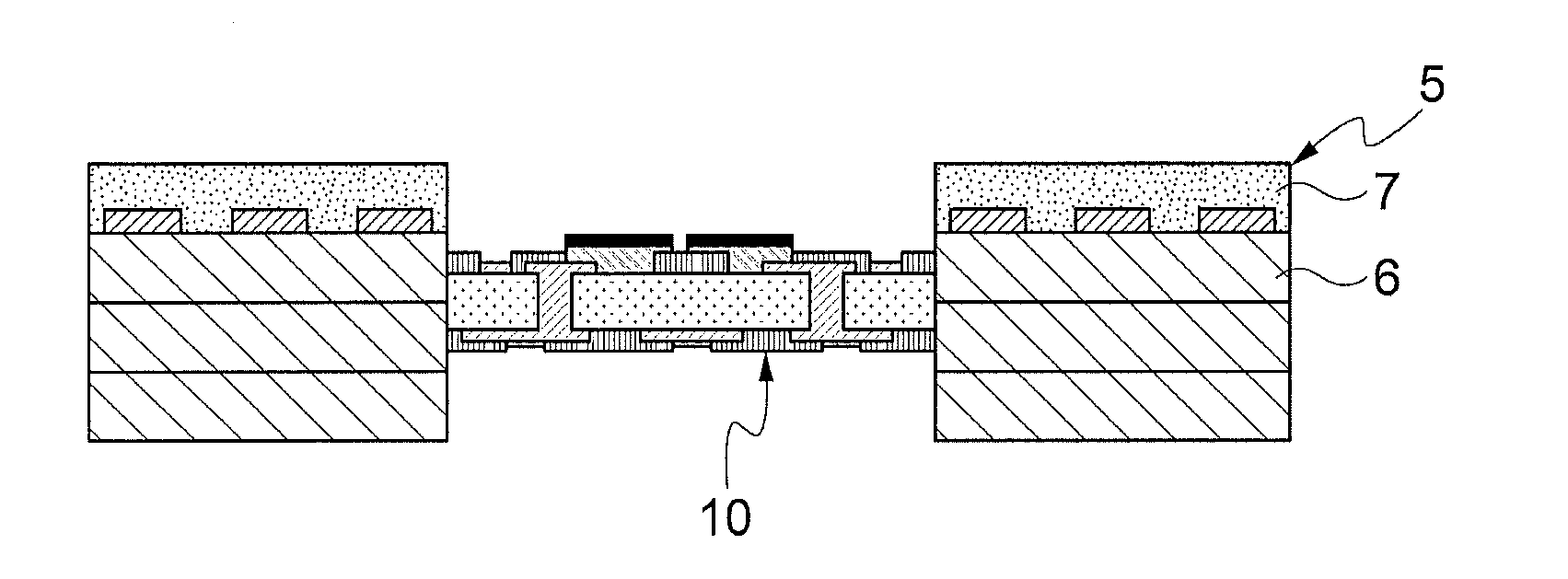
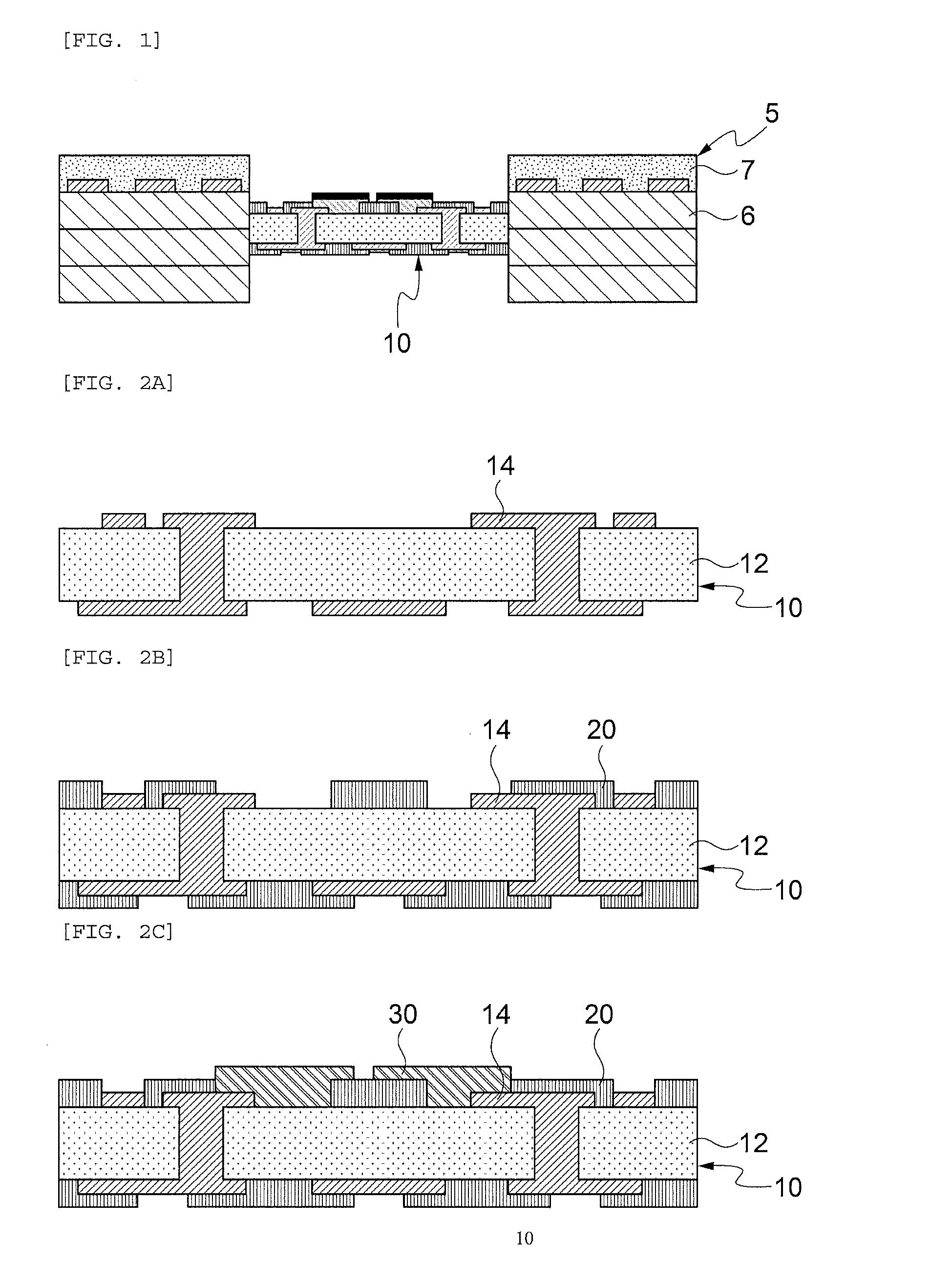
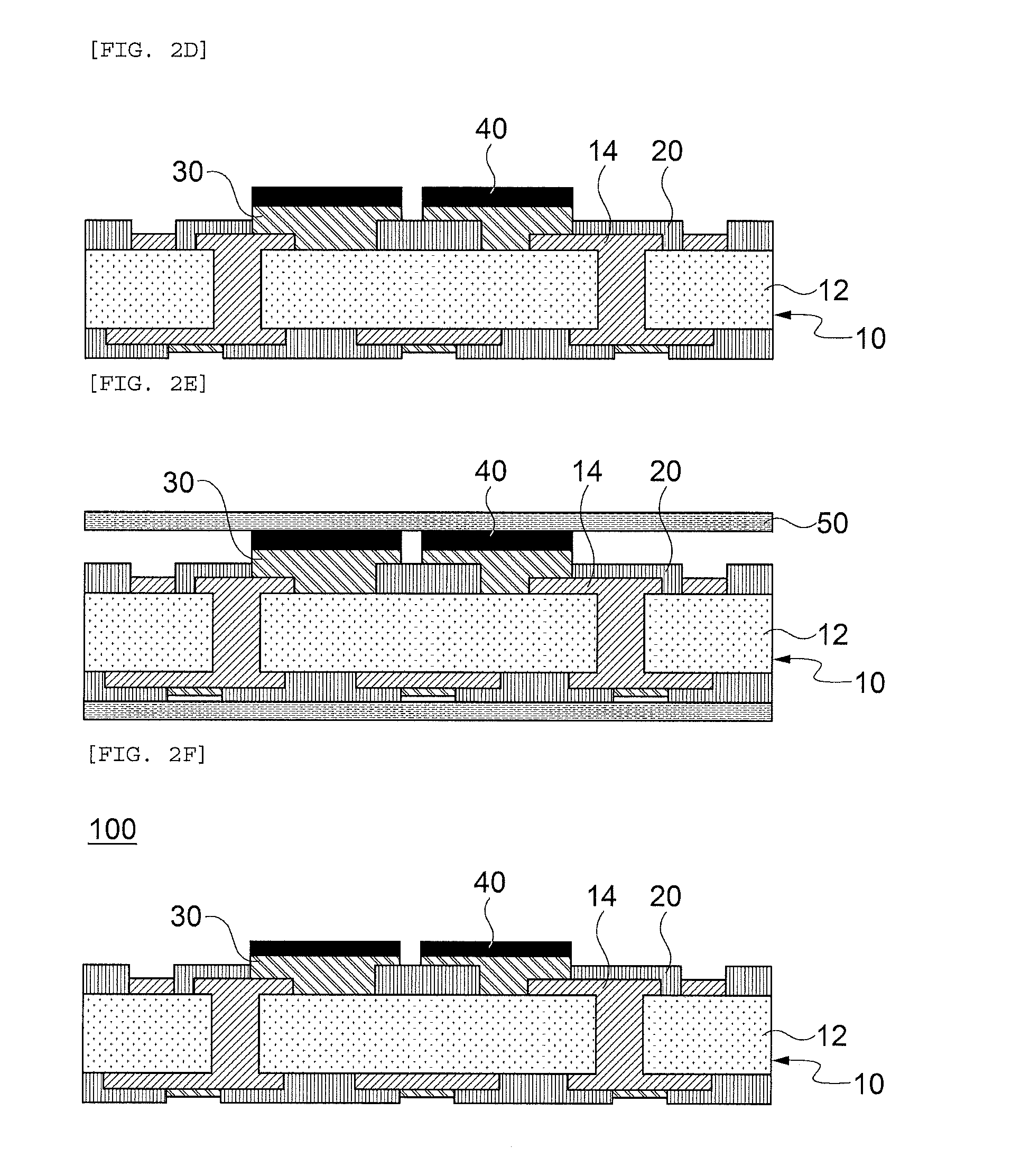
[0022]FIG. 1 is an illustration view showing a printed circuit board according to an exemplary embodiment of the present invention and FIGS. 2A to 2F are illustration views showing processes of manufacturing the printed circuit board according to an exemplar...


PUM

PropertyMeasurementUnit
temperatureaaaaaaaaaa
flexibleaaaaaaaaaa
pressureaaaaaaaaaa

Abstract

Disclosed herein are a printed circuit board and a manufacturing method thereof. The printed circuit board includes a rigid substrate having a solder resist applied thereon and a flexible substrate connected to the rigid substrate in order to increase productivity by simplifying a process of manufacturing the printed circuit board. The manufacturing method includes: attaching a coverlay onto an upper surface of the flexible substrate; attaching an electromagnetic interference (EMI) film onto an upper surface of the coverlay; attaching and pressurizing a substrate molding subsidiary material onto an upper surface of the EMI film; and separating the substrate molding subsidiary material.

Description

CROSS REFERENCE(S) TO RELATED APPLICATIONS[0001]This application claims the benefit under 35 U.S.C. Section 119 of Korean Patent Application Serial No. 10-2013-0080409, entitled “Printed Circuit Board and Manufacturing Method Thereof” filed on Jul. 9, 2013, which is hereby incorporated by reference in its entirety into this application.BACKGROUND OF THE INVENTION[0002]1. Technical Field[0003]The present invention relates to a printed circuit board and a manufacturing method thereof, and more particularly, to a printed circuit board capable of increasing productivity by simplifying a process of manufacturing the printed circuit board and a manufacturing method thereof.[0004]2. Description of the Related Art[0005]Recently, in accordance with portability and high-functionality of an electronic device, and Internet, moving images, and transmission, reception of high capacity data, and the like, a design of a printed circuit board is more complicated and a demand for a high-density and m...

Claims


Application Information

Patent Timeline
Patent Type & Authority Applications(United States)
IPC IPC(8): B32B37/00H05K3/36H05K3/46H05K1/02H05K1/14
CPCH05K3/4611H05K3/361B32B37/00H05K1/028H05K1/148H05K1/0216H05K2201/0723H05K3/4691B32B2307/212B32B2457/08H05K3/28
Inventor PARK, JUN YONGJOUNG, JAE WOO
Owner SAMSUNG ELECTRO MECHANICS CO LTD
Why Eureka
Try Eureka