

Polishing apparatus and polished-state monitoring method
a technology of polishing apparatus and monitoring method, which is applied in the direction of lapping machines, instruments, manufacturing tools, etc., can solve the problems of spectral film thickness monitor, inability to calibrate in-situ, and inability to accurately measure the polishing state, and achieve high-precision polishing results. , the effect of accurate polishing sta
- Summary
- Abstract
- Description
- Claims
- Application Information
AI Technical Summary
Benefits of technology
Problems solved by technology
Method used
Image

Examples
Embodiment Construction
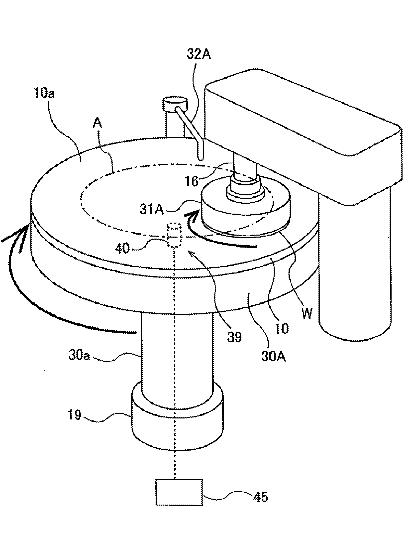
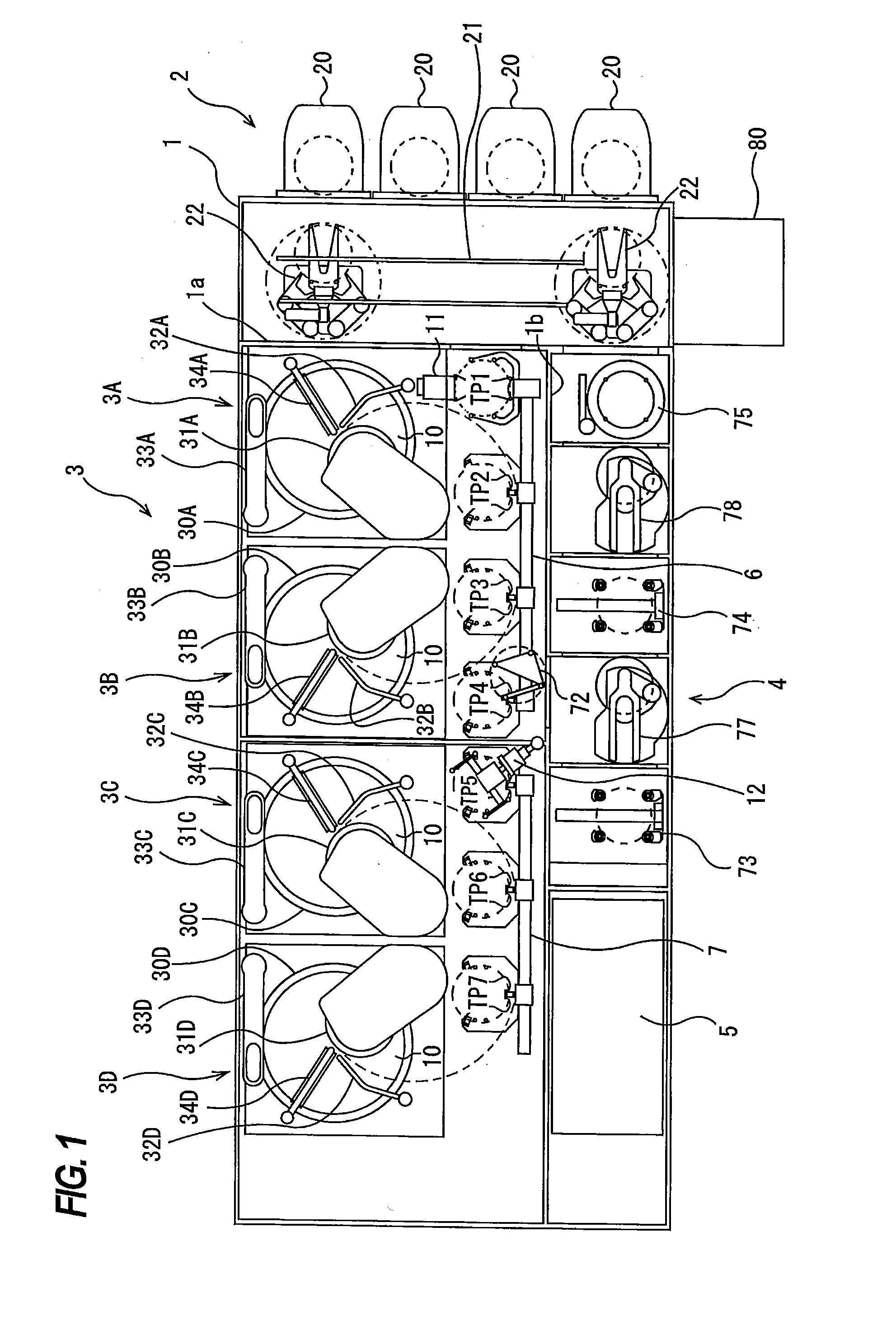
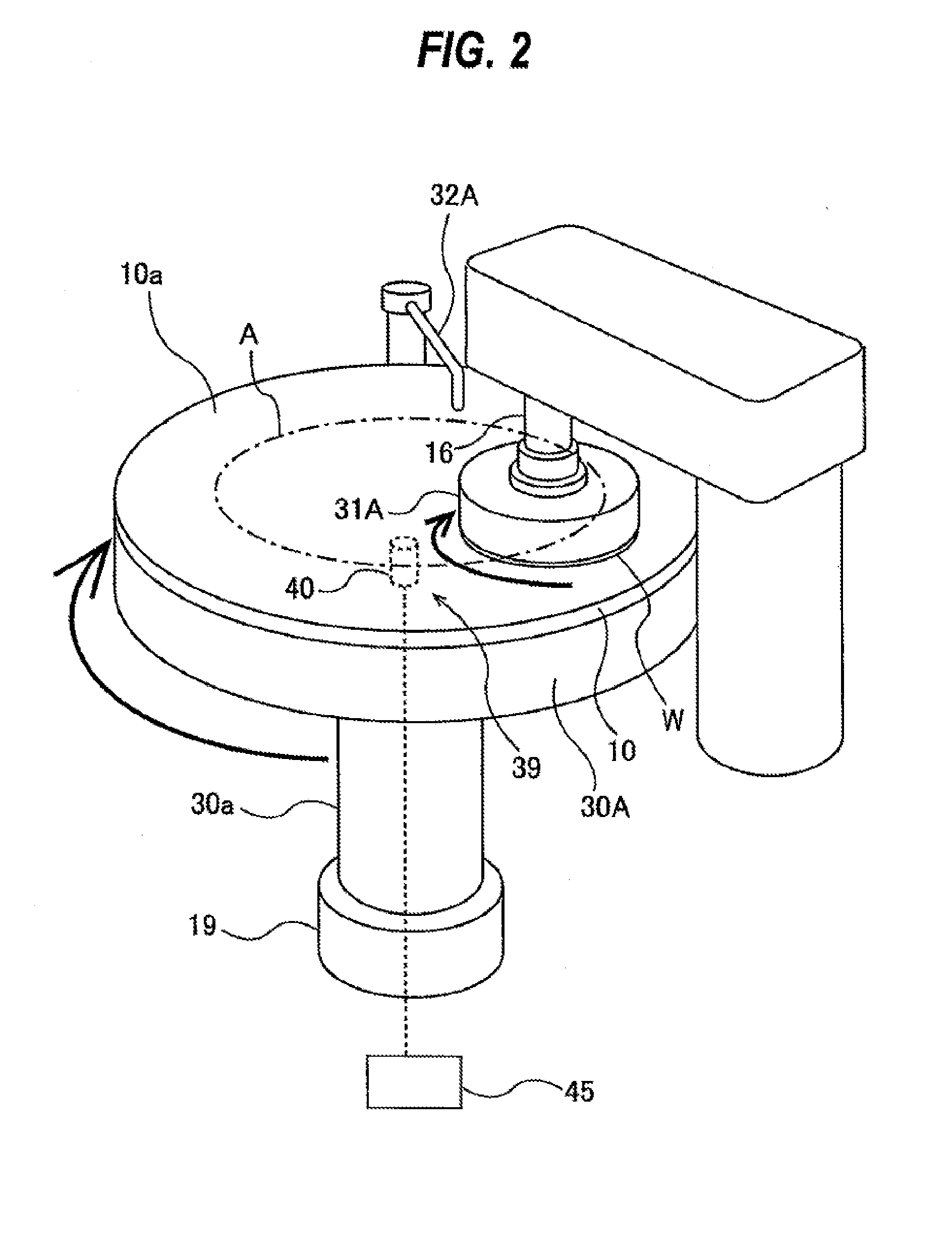
[0036]Embodiments will be described with reference to the drawings. FIG. 1 is a view showing a polishing apparatus according to an embodiment. As shown in FIG. 1, the polishing apparatus has a housing 1 in approximately a rectangular shape. An interior space of the housing 1 is divided by partitions 1a, 1b into a load-unload section 2, a polishing section 3, and a cleaning section 4. The polishing apparatus includes an operation controller 5 configured to control wafer processing operations.
[0037]The load-unload section 2 has front load sections 20 on which wafer cassettes are placed, respectively. A plurality of wafers (or substrates) are stored in each wafer cassette. The load-unload section 2 has a moving mechanism 21 extending along an arrangement direction of the front load sections 20. Two transfer robots (loaders) 22 are provided on the moving mechanism 21, so that the transfer robots 22 can move along the arrangement direction of the front load sections 20. Each transfer rob...
PUM
| Property | Measurement | Unit |
|---|---|---|
| thickness | aaaaa | aaaaa |
| rotational angle | aaaaa | aaaaa |
| thickness distribution | aaaaa | aaaaa |
Abstract
Description
Claims
Application Information