Package structure of an optical module

Inactive Publication Date: 2015-01-29
LINGSEN PRECISION INDS
View PDF6 Cites 5 Cited by
  • Summary
  • Abstract
  • Description
  • Claims
  • Application Information

AI Technical Summary

Benefits of technology

The present invention provides a package structure for an optical module that improves the efficiency of light emitting chips and enhances the reception of light receiving chips. This is achieved by using encapsulating gels with different curvatures to improve the luminous efficiency and reception quality of the chips. The connection region between the gels and the cover is increased through engaging means to enhance the engagement of the package structure.

Problems solved by technology

After the aforementioned conventional optical sensing module is packaged, the power of the light emitted by the light emitting chip of the module reflected by the surface of the object has been greatly reduced so that the light signal received by the adjacent light receiving chip is bad or even cannot be received.
This causes the signal of the recited intelligent electronic devices can not be stable and accurate for interpretation.
Thereby, the light emitting chip and the light receiving chip can be spaced and arranged on the substrate to avoid interference of a light source and reduce product performance.

Method used


Image

  • Package structure of an optical module
  • Package structure of an optical module
  • Package structure of an optical module

Examples


Embodiment Construction

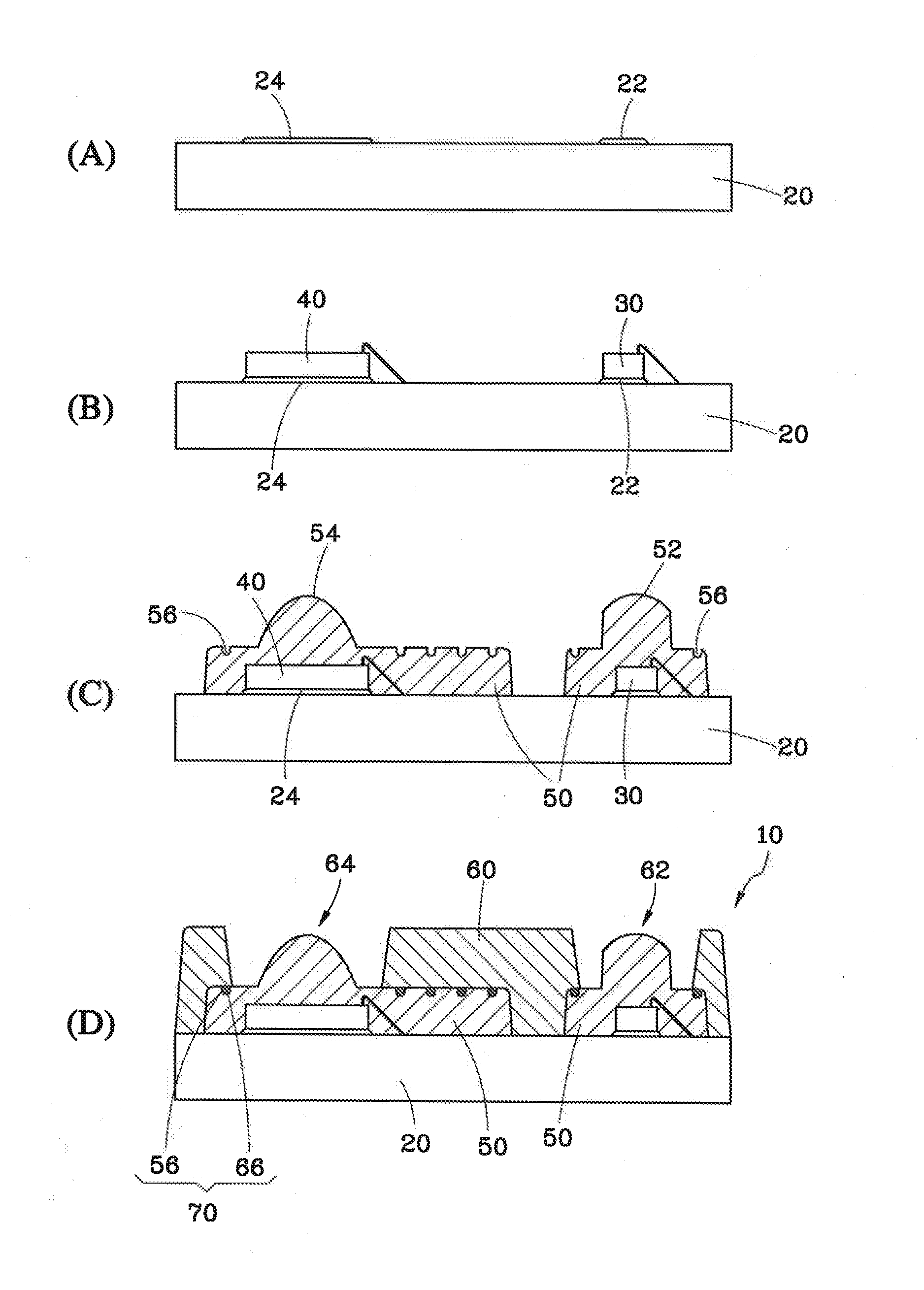
[0029]In order to illustrate the structure, characteristics and effectiveness of the present invention in detail, a preferred embodiment and corresponding diagrams are illustrated as follows.

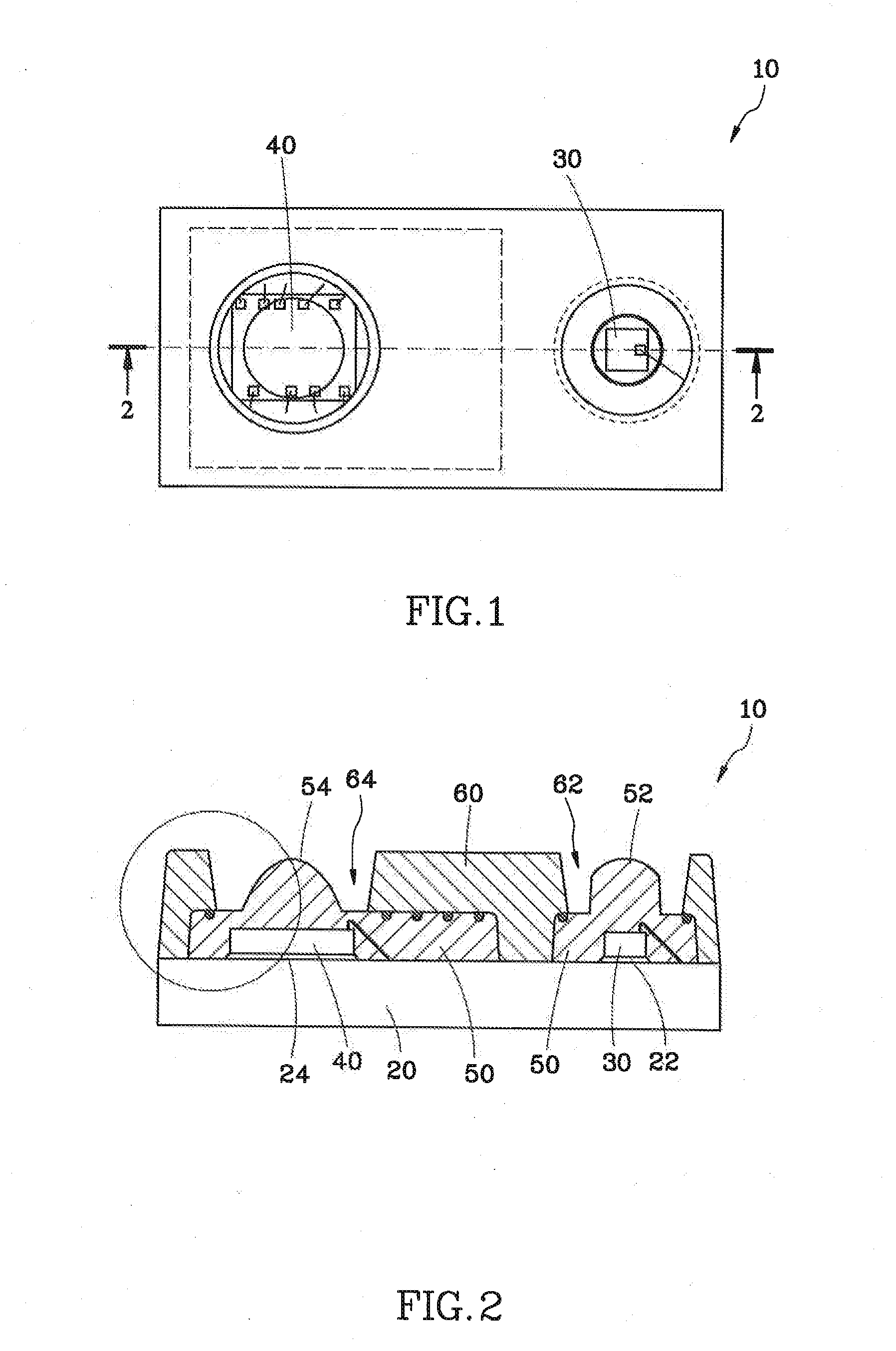
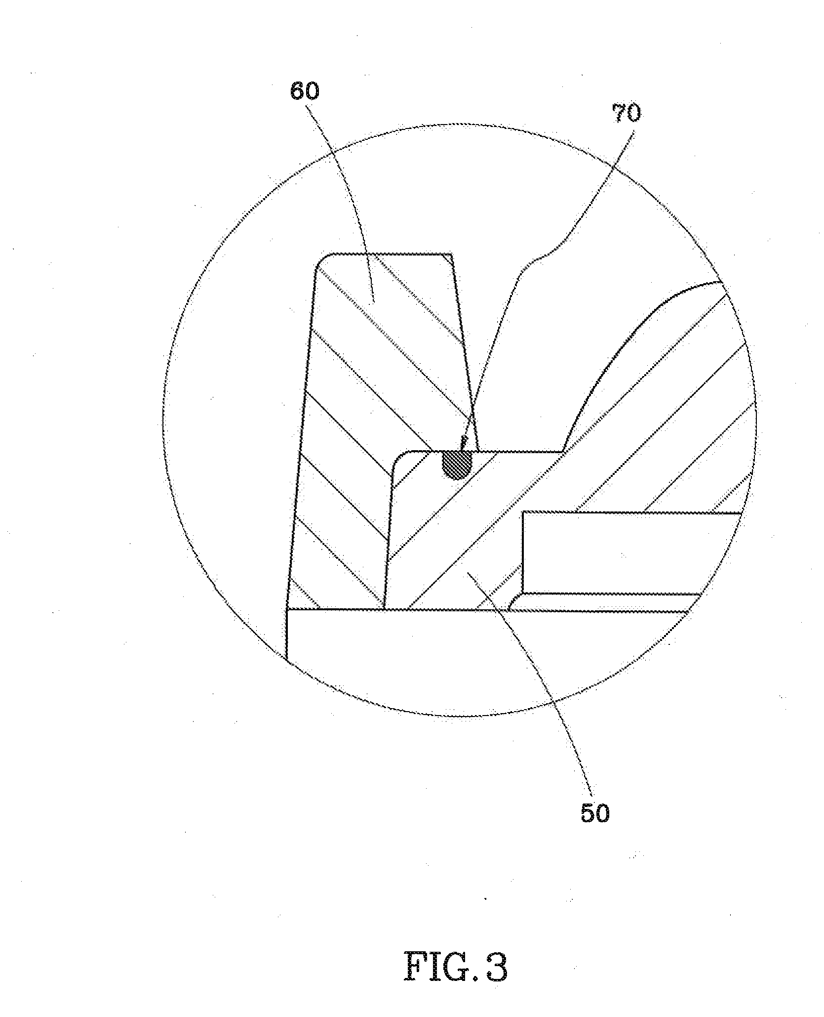
[0030]Please refer to FIG. 1 to FIG. 3, the package structure 10 of an optical module of a preferred embodiment of the present invention is a module cut from a general package array and comprises a substrate 20, a light emitting chip 30, a light receiving chip 40, two encapsulating gels 50, a cover 60, and an engaging means 70.

[0031]The substrate 20 in the preferred embodiment is a non-ceramic substrate, such as a Bismaleimide Triazine (known as BT) substrate or a glass fiber (known as FR4) substrate made of organic materials. Thereby, the material cost of the substrate20 is low. The surface of the substrate 20 defines a light emitting region 22 and a light receiving region 24.

[0032]The light emitting chip 30 and the light receiving chip 40 are treated by a die attaching process and a wire bondi...


PUM


Abstract

This invention relates to a package structure of an optical module. A light emitting and light receiving chips are disposed on a light emitting and light receiving region of the substrate, respectively. Two encapsulating gels cover the light emitting chip and the light receiving chip, respectively, and form a first and a second hemispherical lens portions on the light emitting chip and the light receiving chip, respectively. A cover is affixed on the substrate and each of the encapsulating gels and has a light emitting hole and a light receiving hole, wherein the first and the second lens portions are accommodated, respectively. An engaging means is formed on an adjacent surface between each encapsulating gels and the cover in a horizontal direction. Thereby, the package structure of the optical module of the present invention increases the connection region between each encapsulating gels and the cover to enhance the engagement.

Description

BACKGROUND OF THE INVENTION[0001]1. Field of the Invention[0002]The present invention relates to a package structure, especially related to a package structure of an optical module.[0003]2. Descriptions of the Related Art[0004]Currently, optical proximity sensing modules have become a mainstream technology choice of the new generation of intelligent electronic devices (such as smart phones). When the electronic device is close to someone's ears (face detection) or placed in a pocket, the module will immediately turn off the screen display to save power and prevent accidental screen presses to provide a better user experience. The action principle of the module is emitting a light source with a light emitting chip, such as a light emitting diode (LED), the light is reflected by the surface of an object and is then projected onto a light receiving chip to be converted to electrical signals for subsequent processing. After the aforementioned conventional optical sensing module is packa...

Claims


Application Information

Patent Timeline
IPC IPC(8): H01L25/16H01L25/00
CPCH01L25/50H01L25/167H01L2224/32225H01L2224/48091H01L2224/48227H01L2224/73265H01L33/54H01L2924/181H01L2924/1815H01L24/73H01L2924/00012
Inventor TU, MING-TEYEH, YAO-TING
Owner LINGSEN PRECISION INDS
Why Eureka
Try Eureka