
Eureka
For R&D, Eureka makes reading and utilizing patents & technical documents easy.
Eureka AIR
Designed for self-driven R&D workflows. Generate viable solutions, solve complex R&D challenges, empower your innovation with AI.

Eureka Materials
Designed for material experts only. Revolutionize your material R&D, from search, analyze, to developing new materials.

TechResearch
Generate reliable direction feasibility study reports for your R&D in just a few steps.

TechSeek
Discover and master advanced knowledge NOW. Basics, ideas, possibilities, all at once.

TechMind
As an expert in R&D Theories, TechMind can generates customized viable solutions instantly.

TechRisk
Analyze your overall solution with one click, know your potential R&D risks in advance.

TechMonitor
Get weekly tech updates, stay abreast of the latest tech innovations and key insights.
Mounting and fixing structure for optical fiber of photoelectron device
- Summary
- Abstract
- Description
- Claims
- Application Information
AI Technical Summary
Benefits of technology
Problems solved by technology
Method used
Image

Examples
embodiment 1
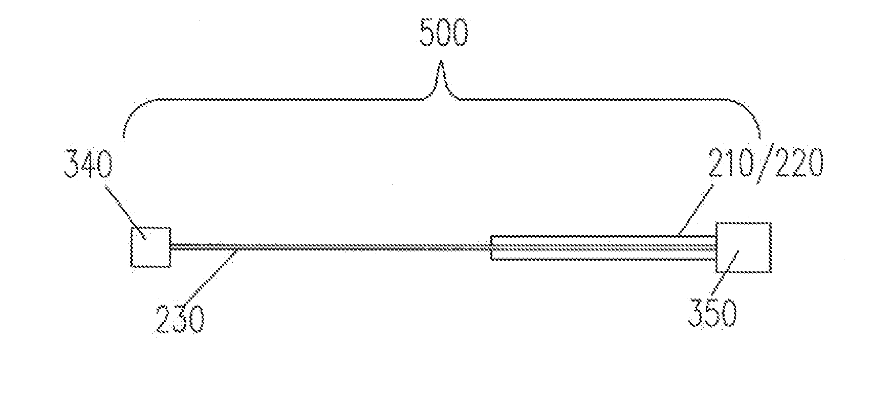
[0042]As shown in FIG. 7a and FIG. 7b, i.e. the schematic diagrams of embodiment 1 of the mounting and fixing structure for an optical fiber of a photoelectron device in the present invention, the mounting and fixing structure includes the above-mentioned non-metalized optical fiber module 500 / 600. Wherein, as shown in FIG. 7a, a stepped hole 141A is fabricated at the opening of a tail tube 140A of the tube body 120, and the ring-shaped preformed low-temperature glass solder 160 having a corresponding size, as shown in FIG. 6, is disposed in the stepped hole 141A; alternatively, as shown in FIG. 7b, a chamfered opening 141B is processed at the opening of a tail tube 140B of the tube body 120, and the ring-shaped preformed low-temperature glass solder 160 having a corresponding size, as shown in FIG. 6, is disposed above the chamfered opening 141B. The non-metalized optical fiber module 500 / 600 penetrates through the tail tube 140A / 140B and the low-temperature glass solder ring 160, ...
embodiment 2
[0047]As shown in FIG. 9a, i.e. the schematic diagram of embodiment 2 of the mounting and fixing structure for an optical fiber of a photoelectron device in the present invention, the mounting and fixing structure includes the foregoing non-metalized optical fiber module 500 / 600. Wherein, a stepped hole 141C is fabricated inside the tail tube 140C of the tube body 120, the stepped hole forms a thin inner tube part of the tail tube 140C towards one side of the tube body 120 and forms a thick inner tube part of the tail tube 140C against one side of the tube body 120; the step refers mainly to the one formed between the stepped hole 141C and the thin inner tube of the tail tube 140C, so that the ring-shaped preformed low-temperature glass solder 160 having a corresponding size, as shown in FIG. 6, can be disposed on the step, whereas the step, as shown in FIG. 9a, may be or may not be arranged between the stepped hole 141C and the thick inner tube of the tail tube 140C; wherein, the t...
PUM
 Abstract
Description
Claims
Application Information
 - R&D Engineer
- R&D Manager
- IP Professional
- Industry Leading Data Capabilities
- Powerful AI technology
- Patent DNA Extraction
Browse by: Latest US Patents, China's latest patents, Technical Efficacy Thesaurus, Application Domain, Technology Topic, Popular Technical Reports.
© 2024 PatSnap. All rights reserved.Legal|Privacy policy|Modern Slavery Act Transparency Statement|Sitemap|About US| Contact US: help@patsnap.com