
Method for reducing lateral extrusion formed in semiconductor structures and semiconductor structures formed thereof

a technology of semiconductor structure and lateral extrusion, which is applied in the field of semiconductor structure, can solve the problems of shorting of active circuit area within the semiconductor structure, slot or void may not prevent shorting in the circuit, and achieve the effect of reducing the lateral extrusion formed

Inactive Publication Date: 2015-02-05
GLOBALFOUNDRIES INC
View PDF0 Cites 6 Cited by
  • Summary
  • Abstract
  • Description
  • Claims
  • Application Information

AI Technical Summary

Benefits of technology

The patent describes a method for reducing a problem called "lateral extrusion" in semiconductor structures. The method involves removing a portion of a layer made of aluminum, and then measuring the thickness of a layer of dielectric material that is placed on top of the aluminum layer. By measuring this difference, the method can help to improve the quality and reliability of semiconductor structures.

Problems solved by technology

The technical problem addressed in this patent text is how to prevent extrusions during the metal annealing process in semiconductor structures, without compromising the size of the active circuit area and requiring new circuit design or larger overall size for electronic devices.

Method used


Image

  • Method for reducing lateral extrusion formed in semiconductor structures and semiconductor structures formed thereof
  • Method for reducing lateral extrusion formed in semiconductor structures and semiconductor structures formed thereof
  • Method for reducing lateral extrusion formed in semiconductor structures and semiconductor structures formed thereof

Examples


Embodiment Construction

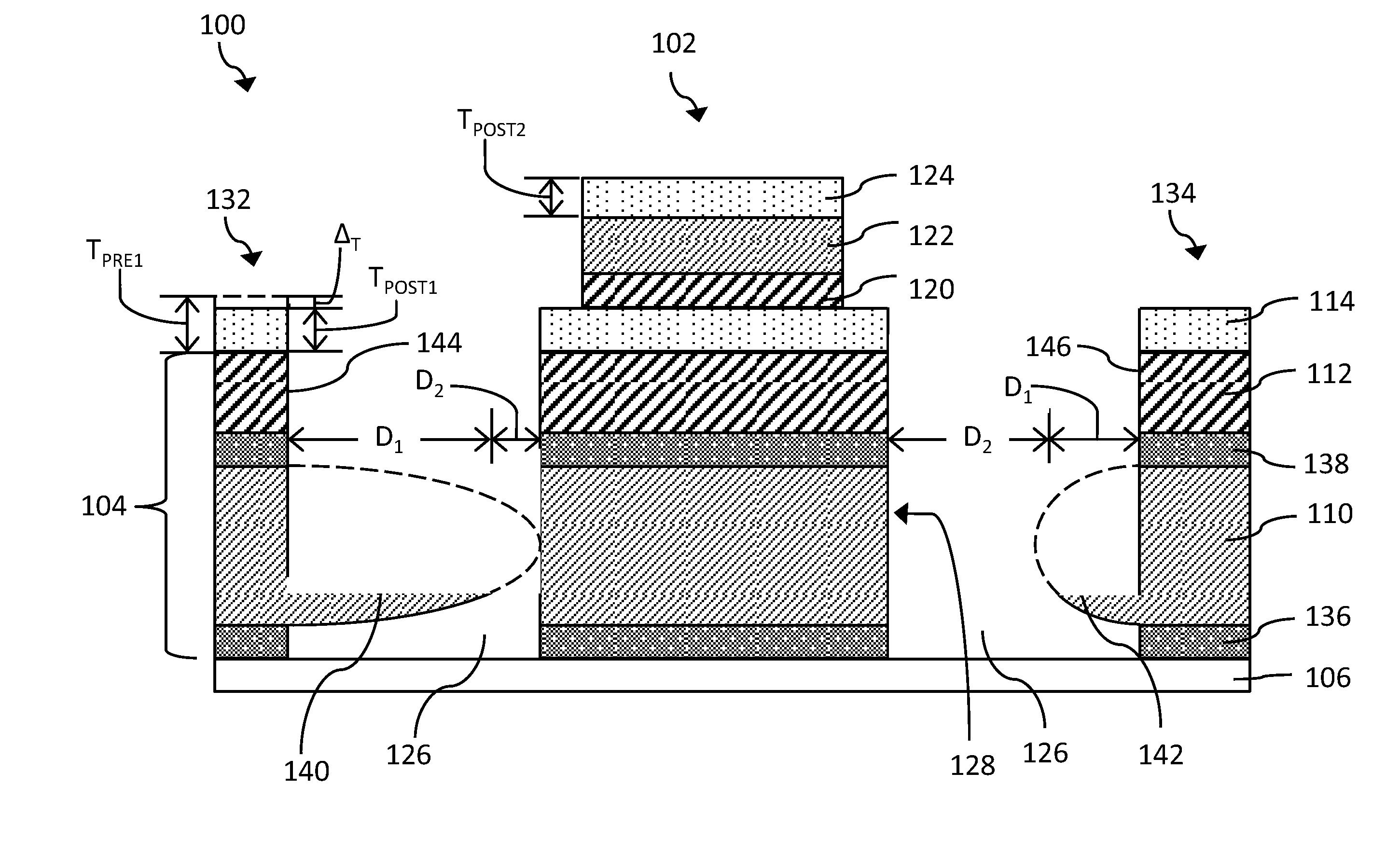
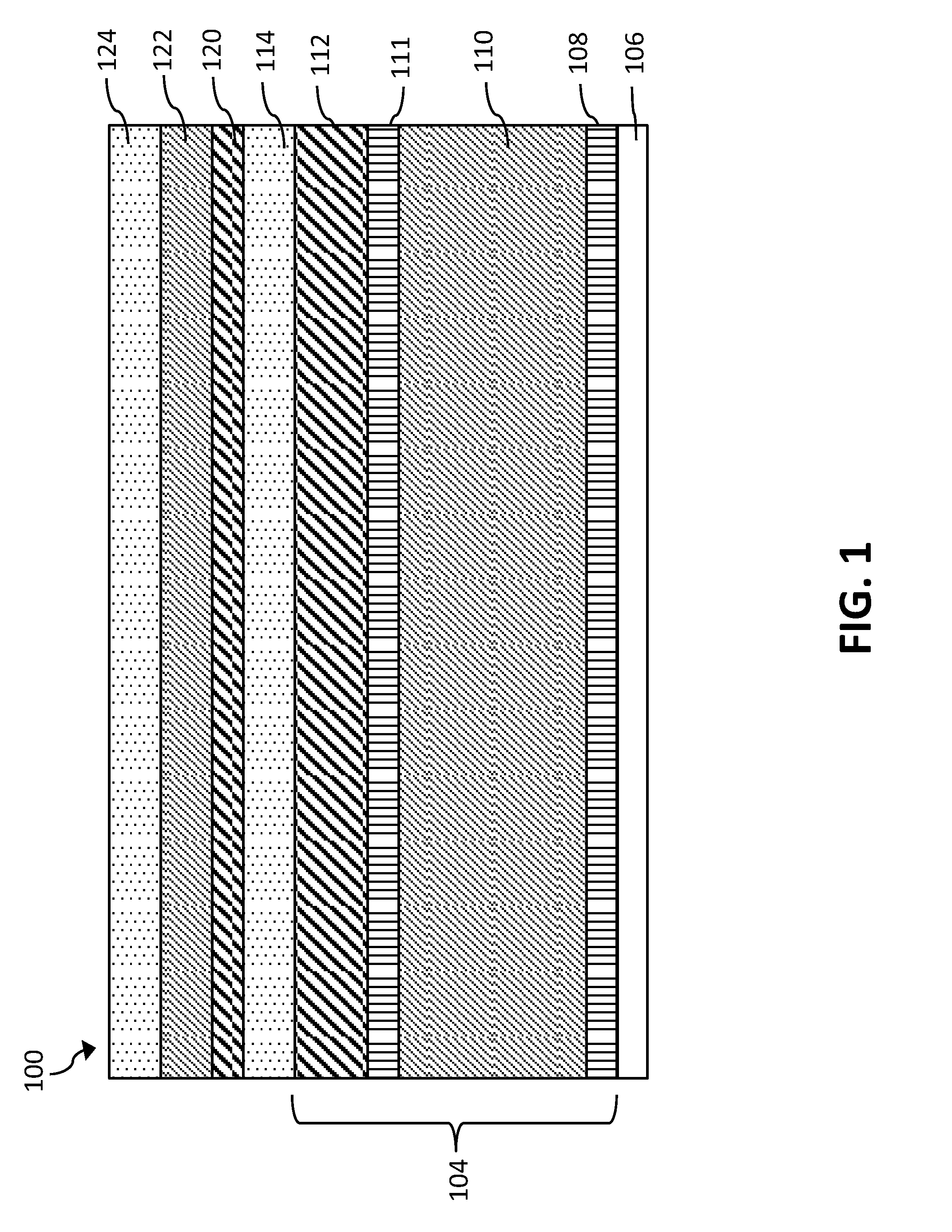
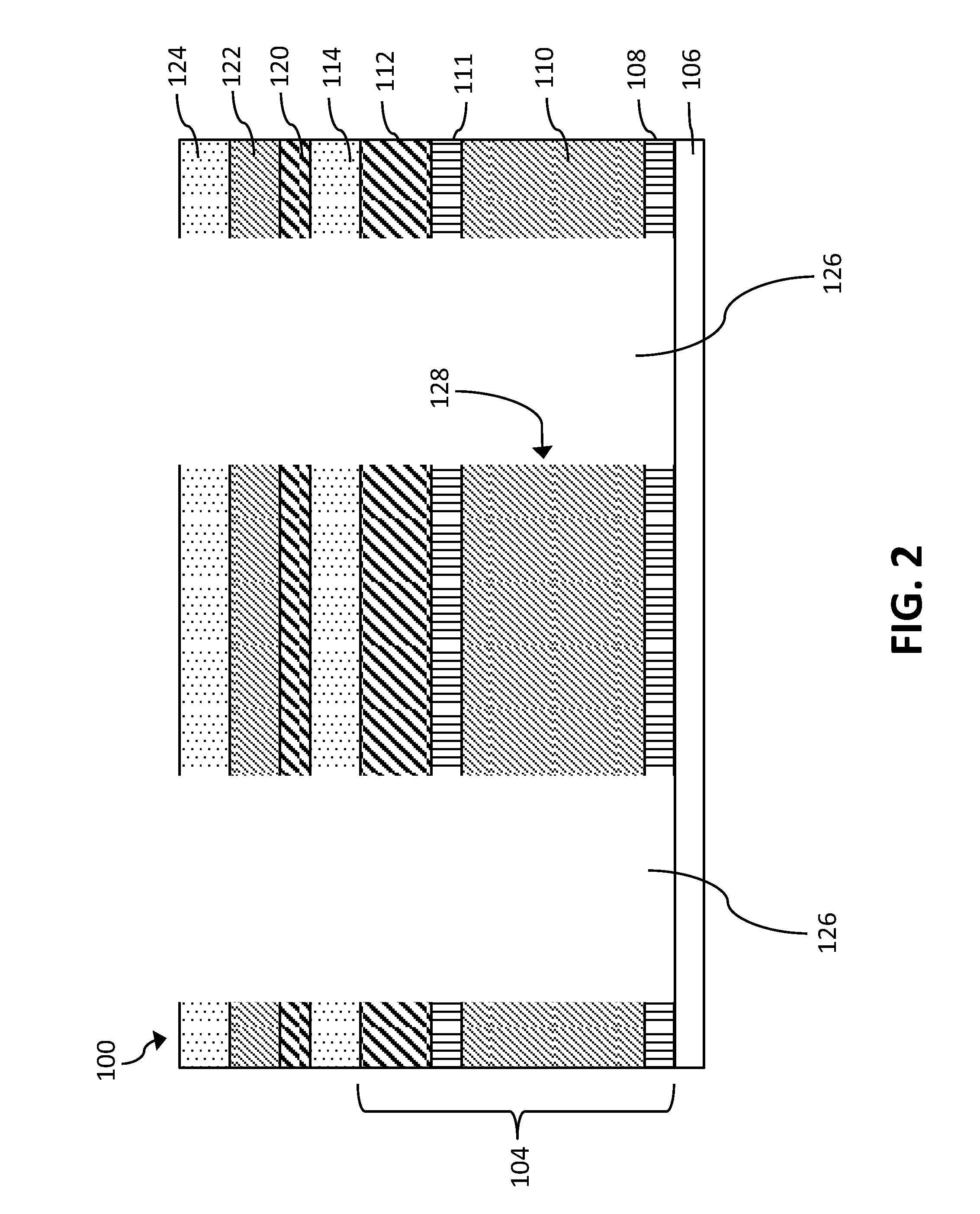
[0014]As described herein, aspects of the invention relate to a method for reducing lateral extrusion formed in semiconductor structures and semiconductor structures formed thereof. Specifically, as described herein, aspect of the invention are related to removing a portion of a lateral extrusion in an aluminum layer of a semiconductor structure. One method of removing a portion of a lateral extrusion in an aluminum layer of a semiconductor structure may now be described. Turning to FIGS. 1-4, one illustrative method according to various embodiments is shown.

[0015]FIG. 1 depicts a process according to various embodiments of the invention, the process including providing a semiconductor structure 100. That is, FIG. 1 shows a cross-section front view of a portion of semiconductor structure 100 according to embodiments of the invention. As shown in FIG. 1, and as discussed herein, semiconductor structure 100 may include a metal-insulator-metal capacitor structure (MIM capacitor) 102 (F...


PUM


Abstract

Aspects of the present invention relate to method for reducing lateral extrusion formed in semiconductor structures and semiconductor structures formed thereof. Various embodiments include a method for reducing lateral extrusion formed in semiconductor structures. The method can include removing a portion of a first lateral extrusion in an aluminum layer of the semiconductor structure, and determining a post-removal thickness of a dielectric layer positioned adjacent the aluminum layer. The post-removal thickness may be determined subsequent to the removing of the portion of the first lateral extrusion. The method can also include determining a difference between the post-removal thickness of the dielectric layer and a pre-removal thickness of the dielectric layer.

Description


Claims


Application Information

Patent Timeline
Owner GLOBALFOUNDRIES INC
Learn More