Sputtered tungsten diffusion barrier for improved interconnect robustness

a technology of diffusion barrier and tungsten, which is applied in the direction of vacuum evaporation coating, semiconductor devices, coatings, etc., can solve the problems of cvd-w stud defects, underlying materials are often attacked, and the surface of this electrically insulative layer is routinely uneven, so as to reduce the extrusion of metal wires, increase the target to substrate distance, and reduce the heating effect

Inactive Publication Date: 2001-06-12
GLOBALFOUNDRIES INC
View PDF22 Cites 13 Cited by
  • Summary
  • Abstract
  • Description
  • Claims
  • Application Information

AI Technical Summary

Benefits of technology

Utilizing non-collimated sputter depositing increases the target to substrate distance inside the sputter chamber than collimated sputter depositing. Non-collimated sputtering reduces the heating effect of traditional collimated sputtering reducing extrusion of metal wires. In addition, non-collimated sputtering provides lower via resistance than collimated sputtering.

Problems solved by technology

The surface of this electrically insulative layer will routinely be uneven due to the uneven underlying contour of the patterned conductive layer.
However, during CVD-W to fill the via, the underlying materials are often attacked by the chemicals used in the CVD process.
Robustness of the diffusion barrier is important since failure of the barrier films result in attack of the underlying structures and / or defects in the CVD-W stud.
Despite significant improvements in the barrier film quality, failure of these barriers is still a serious problem in semiconductor manufacture.
However, it has been found that during collimation tremendous energy is created which is transferred to the silicon wafer of the semiconductor device.
Temperatures exceeding 420.degree. C. are possible leading to extrusion of the aluminum lines.
Non-collimated sputtering reduces the heating effect of traditional collimated sputtering reducing extrusion of metal wires.
In addition, non-collimated sputtering provides lower via resistance than collimated sputtering.

Method used


Image

  • Sputtered tungsten diffusion barrier for improved interconnect robustness
  • Sputtered tungsten diffusion barrier for improved interconnect robustness
  • Sputtered tungsten diffusion barrier for improved interconnect robustness

Examples


Embodiment Construction

)

In describing the preferred embodiment of the present invention, reference will be made herein to FIGS. 1-6 of the drawings in which like numerals refer to like features of the invention. Features of the invention are not necessarily shown to scale in the drawings.

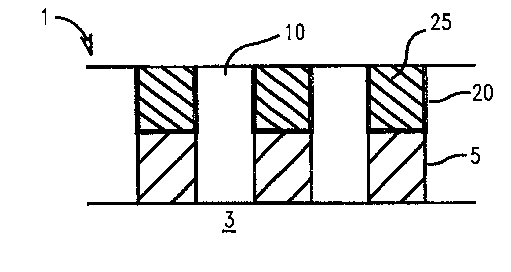
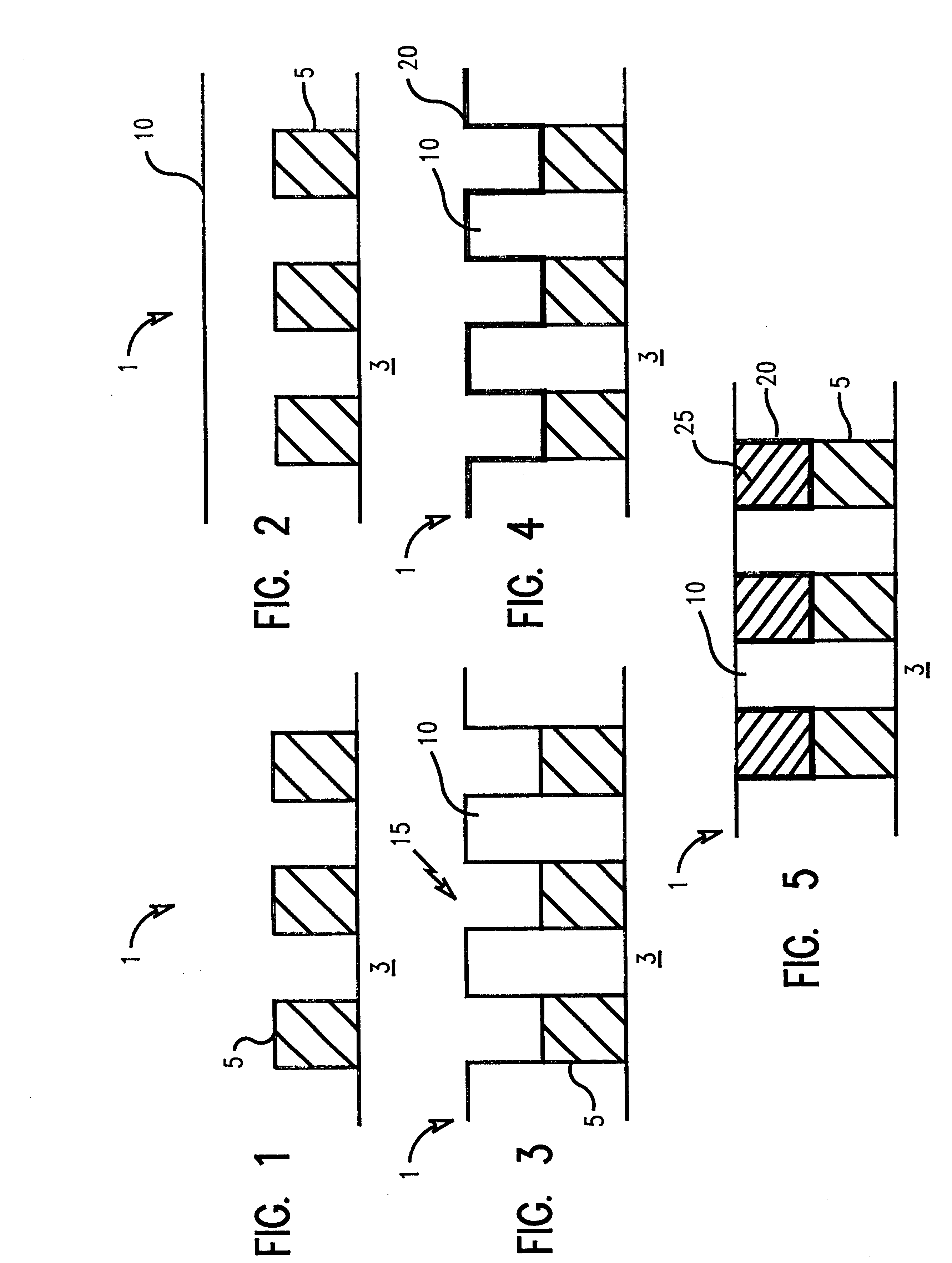
In FIG. 1, semiconductor device 1 has a substrate 3 shown with multiple metal lines 5 formed on its surface. Substrate 3, typically made of silicon, not only includes metal lines 5 as shown. It may also include a plurality of dielectric and conductive layers, such as silicon oxide or nitride, as are necessary to form active devices on a semiconductor substrate. Metal lines are typically low resistivity metals such as aluminum or copper, and their binary and tertiary alloys. They are generally deposited using physical vapor deposition, patterned, and etched to produce the desired circuitry. The metal lines 5 can also be connected to an electrically active device in substrate 3 (not shown).

FIG. 2 shows continued processing ...


PUM

PropertyMeasurementUnit
thicknessaaaaaaaaaa
pressureaaaaaaaaaa
thicknessaaaaaaaaaa

Abstract

A method of forming inter-level contacts or vias between metal layers using a tungsten film deposited into the via using non-collimated sputter deposition. The sputter chamber is configured with a pressure of about 1 mTorr to about 10 mTorr with an inert gas flow of at least at least 25 cm3/min to about 150 cm3/min. Shielding inside the chamber is coated with a material, preferably, aluminum oxide, that promotes adhesion of tungsten to the shielding. An adhesion layer of titanium may be included prior to deposition of the tungsten film. Non-collimated sputter deposition increases the target to substrate distance inside the sputter chamber; reduces the heating effect associated with traditional collimated sputtering; and provides more robust diffusion barriers.

Description

1. Field of the InventionThe present invention relates to semiconductor devices, and more particularly, to a method of sputtering tungsten diffusion barriers in contact and via holes in semiconductor devices having increased robustness.2. Description of Related ArtIn the manufacture of semiconductor devices, metal conductive layers are patterned for the purpose of making interconnections between different points on the device. After formation of this patterned metal conductive layer, an electrically insulative material such as silicon dioxide or silicon nitride is deposited over the metal conductive layer by conventional deposition techniques. The surface of this electrically insulative layer will routinely be uneven due to the uneven underlying contour of the patterned conductive layer. The presence of a metal interconnect path beneath the insulative layer results in a corresponding elevated path in the surface contour of the insulative layer.Often it is necessary, especially in hi...

Claims


Application Information

Patent Timeline
Patent Type & Authority Patents(United States)
IPC IPC(8): C23C14/56C23C14/04C23C14/16H01L21/02H01L21/70H01L21/285H01L21/768H01L21/28
CPCC23C14/046C23C14/165C23C14/564H01L21/2855H01L21/76843H01L21/76876H01L21/28
Inventor BRODSKY, STEPHEN B.MURPHY, WILLIAM J.RUTTEN, MATTHEW J.STRIPPE, DAVID C.VANSLETTE, DANIEL S.
Owner GLOBALFOUNDRIES INC
Why Eureka
Try Eureka