

Large-area and low-power laser stripping method for GaN-base epitaxial layer
A laser lift-off and epitaxial layer technology, applied in lasers, semiconductor lasers, laser welding equipment, etc., can solve problems such as poor electrical and thermal conductivity of sapphire hardness, limited crystal quality of GaN-based materials, and complex material growth processes, etc., to ensure integrity Uniformity, reduced energy density requirements, and the effect of relaxing the spot size
- Summary
- Abstract
- Description
- Claims
- Application Information
AI Technical Summary
Problems solved by technology
Method used
Image

Examples
Embodiment 1
[0033] The technical scheme of embodiment one:
[0034] 1. Adhere the P side of the GaN-based epitaxial wafer on the sapphire substrate to the support substrate such as glass, Si, Cu, etc. with epoxy resin, and place it in a vacuum chamber to remove the air bubbles in the glue to ensure that the epitaxial wafer and the support substrate are stable. Indicates uniform intimate contact without voids.
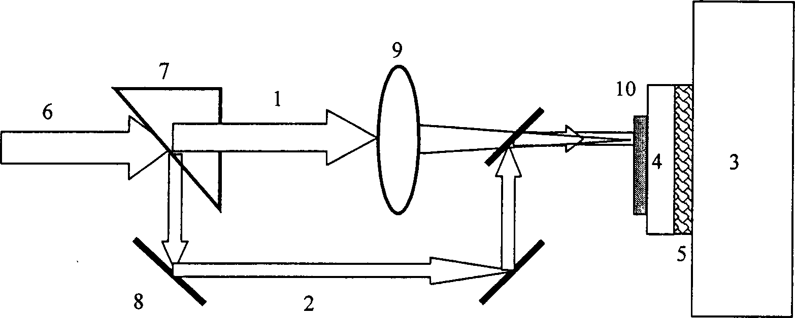
[0035] 2. Adjust the optical path of the excimer laser, such as figure 1 As shown, two beams are irradiated at the same time. The laser pulse 6 is divided into two beams by the beam splitter 7. The beam 1 is the focused beam obtained by passing the beam split by the beam splitter 7 through the focusing lens 9. The beam is caused by the decomposition of GaN at the interface. the main reason. The other beam is the bias beam, which is obtained by passing the light split by the beam splitter 7 through the reflector 8. The bias beam 2 has a larger spot and a smaller energy density, an...
Embodiment 2
[0039] The technical scheme of embodiment two:
[0040] 1. Adhere the P side of the GaN-based epitaxial wafer on the sapphire substrate to the support substrate such as glass, Si, Cu, etc. with epoxy resin, and place it in a vacuum chamber to remove the air bubbles in the glue to ensure that the epitaxial wafer and the support substrate are stable. Indicates uniform intimate contact without voids.
[0041] 2. Heat the sample with an electric heater 5 or local infrared heating of the sample environment, with a temperature range of 0-300°C
[0042] 3. Irradiating the heated sample with an excimer pulsed laser with sufficient energy density, and performing laser lift-off to separate the GaN epitaxial layer 11 from the sapphire substrate 12 .
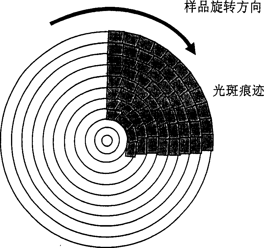
[0043] 4. The sample stage adopts a spiral or arc stepping method during laser peeling, such as figure 2 . The angle of the helix is 0-360°.
[0044] 5. After the laser scans the sample 10, first soak the sample with hot water higher...
Embodiment 3
[0046] The technical scheme of embodiment three:
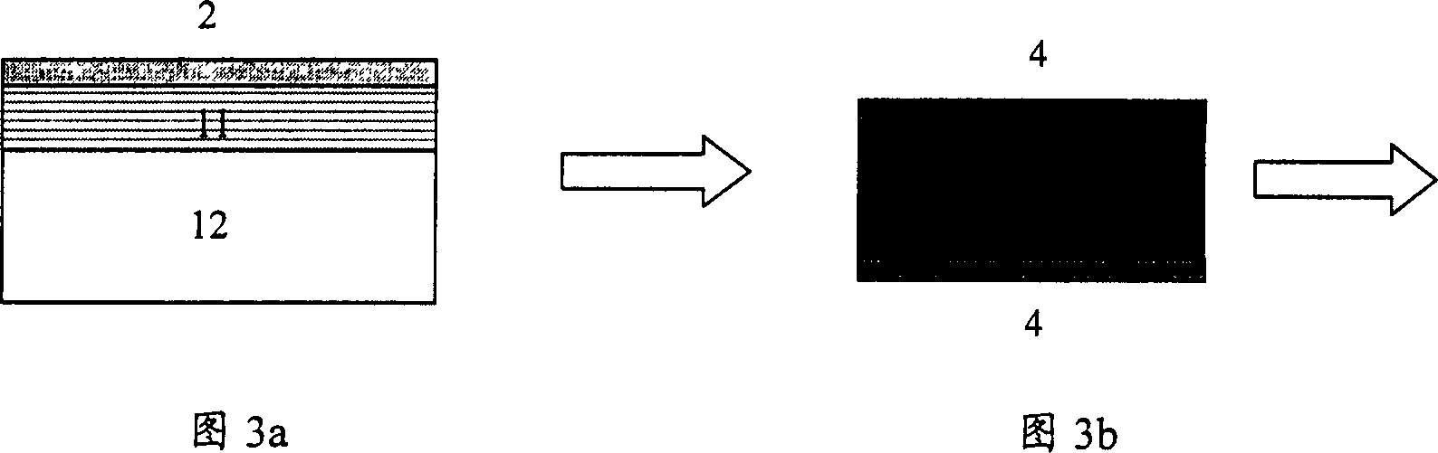
[0047] 1. First prepare a large-area P-type ohmic contact electrode directly on the GaN-based epitaxial layer 11 on the sapphire substrate 12, such as vapor-depositing Ni / Au transparent electrode 1, and then alloy it at 500 ° C under oxygen: nitrogen = 1: 1 5 minutes. For epitaxial wafers with LED structures, a reflective layer of Ti / Ag / Ti / Au needs to be added, as shown in Figure 3a. Among them, " / " is the separation symbol between metal layers, such as Ni / Au means two layers of metal, the first layer is metal Ni, the second layer is metal Au, Ti / Ag / Ti / Au means multi-layer metal film, in turn They are metal Ti, Ag, Ti, Au respectively.
[0048] 2. Prepare Ti / Al / Ti / Au ohmic contact electrodes 4 on the upper and lower surfaces of the cleaned n-type highly doped Si substrate 3, as shown in FIG. 3b.
[0049] 3. On the ohmic contact electrode 4 of GaN ohmic contact electrode 1 and Si substrate 3 sides, sputter metal Ni barrier l...
PUM
 Abstract
Description
Claims
Application Information