PNP light emitting transistor and method

a light-emitting transistor and light-emitting transistor technology, applied in the field of semiconductor devices and methods, to achieve the effect of reducing the amount of acceptor-doped crystal required, reducing the resistance loss in the base region, and reducing the amount of free carrier absorption

Active Publication Date: 2007-08-30
THE BOARD OF TRUSTEES OF THE UNIV OF ILLINOIS
View PDF30 Cites 37 Cited by
  • Summary
  • Abstract
  • Description
  • Claims
  • Application Information

AI Technical Summary

Benefits of technology

[0008] For some applications, it may be desirable that a transistor laser be a pnp HBT rather than an npn HBT, assuming this leads to lower base region resistive loss (which is driven by lateral base currents) and, in addition, assuming lower free carrier absorption (NDONOR<NACCEPTOR) since the base is located largely in the high field active region. In such applications we prefer to put heavily doped p-type crystal outside of the base region and to some extent outside of the high field active region of the transistor laser. Accordingly, one of the features of the invention is to devise an improved HBT laser, and to minimize the amount of acceptor-doped crystal required in the p-type emitter and in the high field p-type collector, by making these regions relatively thin and contacting them via tunnel junctions (i.e., p+ region contacted by n+ region to minimize the total thickness of p-type emitter and collector). [The “+” notation conventionally means “heavily doped”, and, for purposes hereof, is generally donor impurity concentration of at least about 1018 / cm3 for n+, and acceptor impurity concentration of at least about 1019 / cm3 for p+.] In accordance with a feature of the invention, a pnp HBT light emitter is made with just enough p-type crystal to render operative the emitter (hole injection) function and the carrier collector function. That is, the current of the device is carried, to the extent possible, in higher mobility n-type crystal and not lower mobility p-type crystal, thereby minimizing resistive loss.
[0013] The pnp transistor laser can have a number of advantages as compared to the npn transistor laser, as follows: (1) Lower base doping, with resultant reduction in free carrier absorption, lower lasing threshold, and reduced self-heating in the base region, as well as improved QW recombination spectra. (2) Lower base sheet resistance due to superior electron mobility, with accordant improvement in upper base current injection limit, higher power operation, reduced resistive heating in the base region, and also improved base current distribution under the emitter, resulting in lower lasing threshold and reduced edge heating. (3) Lower contact resistance, with resulting reduction in heating effect.
[0014] On top of the listed advantages, the present invention, employing the described tunnel junctions in the pnp transistor laser, can have a number of further advantages, as follows: (1) Reduced contact resistance to emitter and collector contact layers, resulting in reduced heating effect and reduced capacitive effect. (2) Lower collector sheet resistance, resulting in reduced heating effect and higher upper power (collector current×VCE) limit for collector current. (3) Lower series resistance through the emitter cladding layer, and accordant reduction of heating effect. (4) Lower free carrier absorption in the upper and lower cladding region (by minimization of highly doped P− region), resulting in reduced free carrier absorption, and accordant lower lasing threshold and reduced heating effect. It is recognized that the pnp HBT laser may not operate as at high a speed as a super high speed npn HBT, but it can still be an extremely high speed transistor laser with relatively lower current threshold and relatively higher collector voltage breakdown.

Problems solved by technology

However, the problems in the present situation have different aspects, since a bipolar transistor is involved.

Method used


Image

  • PNP light emitting transistor and method
  • PNP light emitting transistor and method
  • PNP light emitting transistor and method

Examples


Embodiment Construction

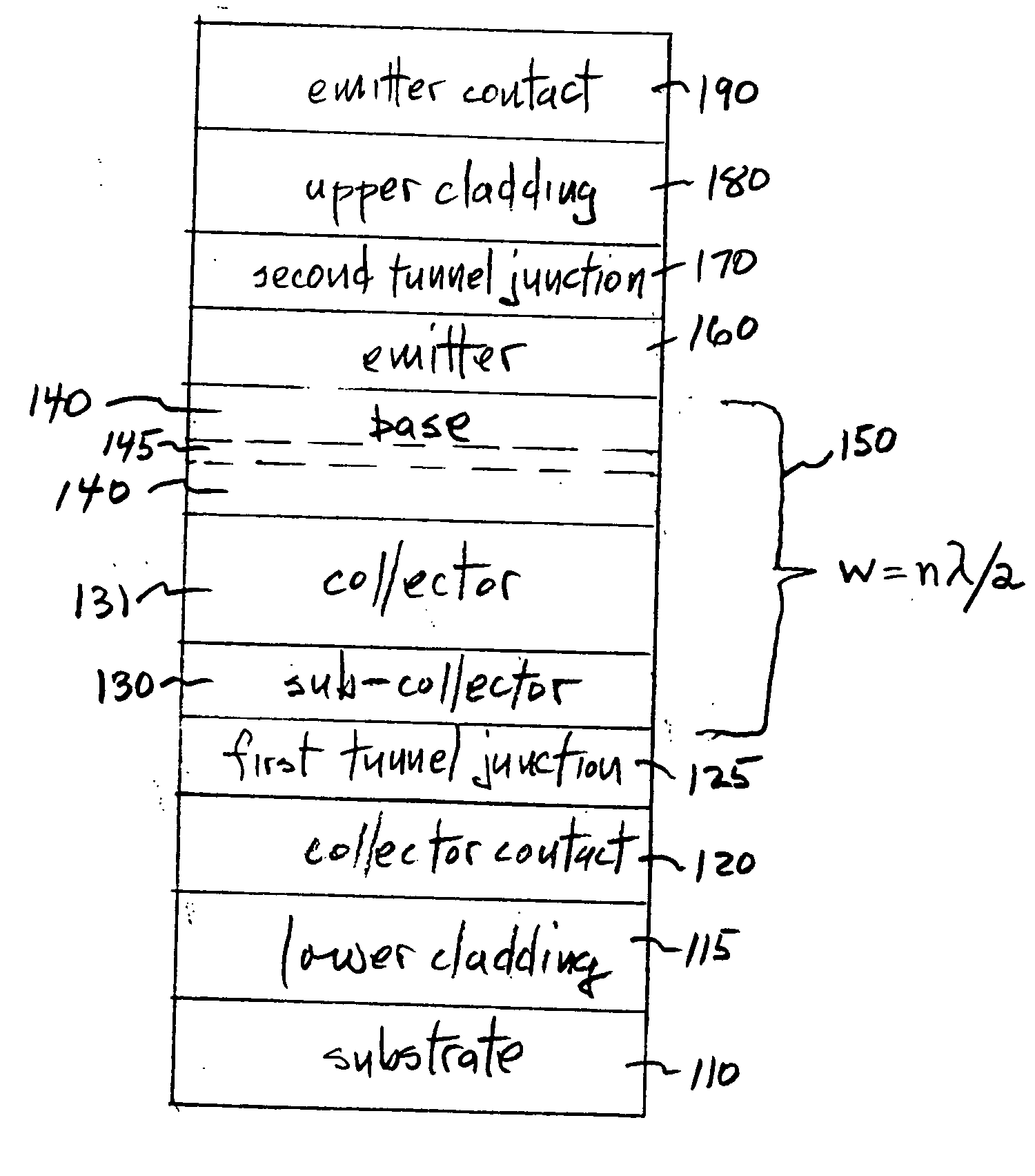
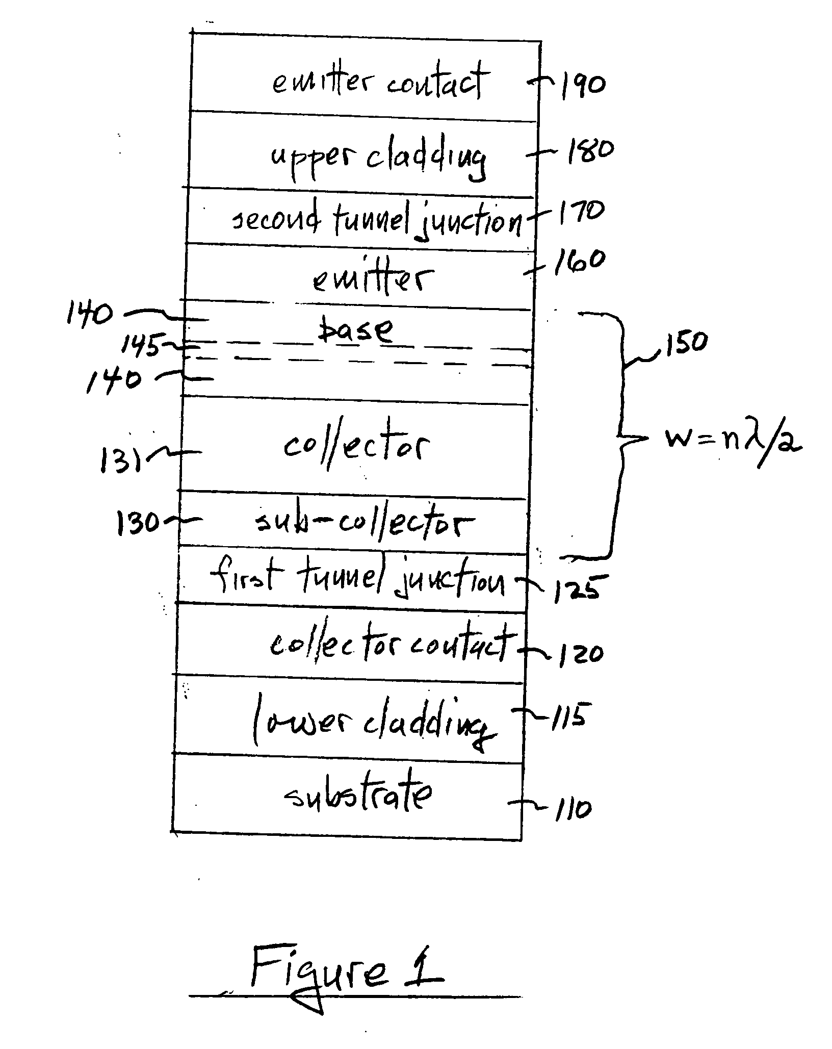
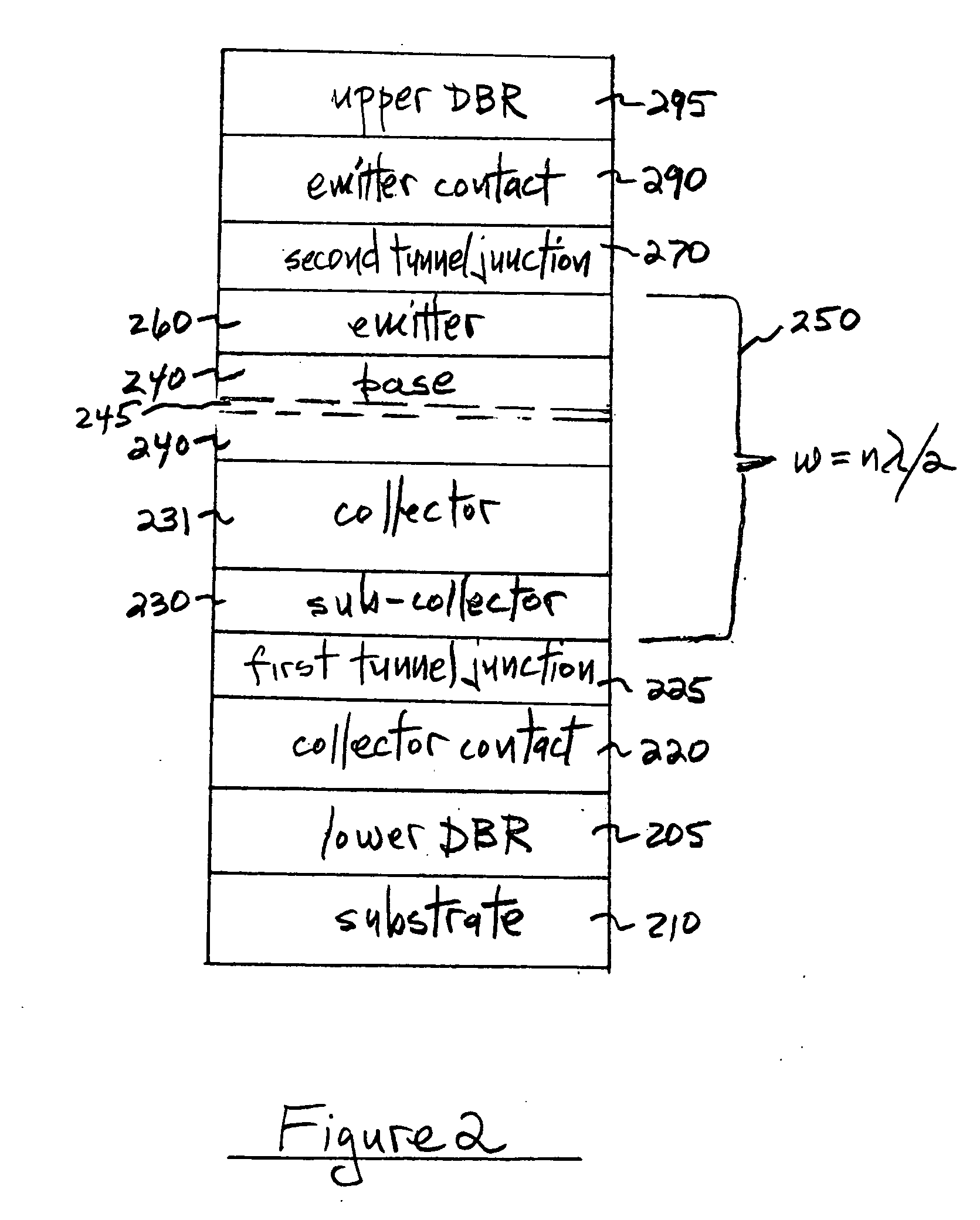
[0020]FIG. 1 is a simplified diagram of the layer structure for an embodiment of the invention. The substrate 110 can be undoped or doped, and has deposited thereon n-type cladding layer 115, n-type collector contact layer 120, a first tunnel junction 125, p-type sub-collector 130 and collector 131 (which can be intrinsic or lightly doped p-type), n-type base 140 containing at least one quantum size layer 145 (e.g. quantum well and / or quantum dot layer(s)), p-type emitter 160, second tunnel junction 170, n-type upper cladding layer 180, and n-type emitter contact layer 190. When this FIG. 1 embodiment is employed as an edge-emitting p-n-p heterojunction bipolar transistor (HBT) laser, the waveguide region (bracket 150) can be enclosed in an optical resonant cavity of width w equal to nλ / 2, with n=1,2,3 . . . , and λ the characteristic emission wavelength. Note that the tunnel junctions 125 and 170 are preferably outside the active base region. In this embodiment, the first tunnel ju...


PUM


Abstract

A semiconductor light-emitting transistor device, including: a bipolar pnp transistor structure having a p-type collector, an n-type base, and a p-type emitter; a first tunnel junction coupled with the collector, and a second tunnel junction coupled with the emitter; and a collector contact coupled with the first tunnel junction, an emitter contact coupled with the second tunnel junction, and a base contact coupled with the base; whereby, signals applied with respect to the collector, base, and emitter contacts causes light emission from the base by radiative recombination in the base.

Description

GOVERNMENT SUPPORT [0001] This invention was made with Government support under Contract Number HR0011-04-1-0034 awarded by the Defense Advanced Research Projects Agency (DARPA). The Government has certain rights in the invention.FIELD OF THE INVENTION [0002] This invention relates to semiconductor devices and methods, and also to PNP bipolar transistors, PNP bipolar light emitting transistors, and PNP bipolar transistor lasers. BACKGROUND OF THE INVENTION [0003] As described, for example, in PCT International Publication Number WO 2005 / 020287A2, and several publications [see, for example, M. Feng, N. Holonyak, Jr., and W. Hafez, “Light-Emitting Transistor: Light Emission From InGaP / GaAs Heterojunction Bipolar Transistors”, Appl. Phys. Lett. 84, 151(2004); M. Feng, N. Holonyak, Jr., and R. Chan, “Quantum-Well-Base Heterojunction Bipolar Light-Emitting Transistor”, Appl. Phys. Lett. 84, 1952 (2004); M. Feng, N. Holonyak, Jr., B. Chu-Kung, G. Walter, and R. Chan, “Type-II GaAsSb / InP H...

Claims


Application Information

Patent Timeline
Patent Type & Authority Applications(United States)
IPC IPC(8): H01S5/00H01L31/00H01L33/00H01L33/04
CPCH01L33/0004H01L33/04H01S5/0421H01S5/3095H01S5/183H01S5/3054H01S5/06203
Inventor WALTER, GABRIELHOLONYAK, NICK JR.FENG, MILTONCHAN, RICHARD
Owner THE BOARD OF TRUSTEES OF THE UNIV OF ILLINOIS
Why Eureka
Try Eureka