Semiconductor memory device

Active Publication Date: 2015-02-19
SK HYNIX INC
View PDF6 Cites 0 Cited by
  • Summary
  • Abstract
  • Description
  • Claims
  • Application Information

AI Technical Summary

Benefits of technology

[0007]Various embodiments relate to a semiconductor m

Problems solved by technology

Two-dimensional memory devices in which memory cells are fabricated in a single layer over a silicon substrate have reached physical limits in increasi

Method used


Image

  • Semiconductor memory device
  • Semiconductor memory device
  • Semiconductor memory device

Examples


Example

[0022]Hereinafter, various embodiments of the present invention will be described with reference to the accompanying drawings. In the drawings, a thicknesses and a distance of components are exaggerated compared to an actual physical thickness and interval for convenience of illustration. In the following description, detailed explanation of known related functions and constitutions may be omitted to avoid unnecessarily obscuring the subject manner of the present invention. Like reference numerals refer to like elements throughout the specification and drawings.

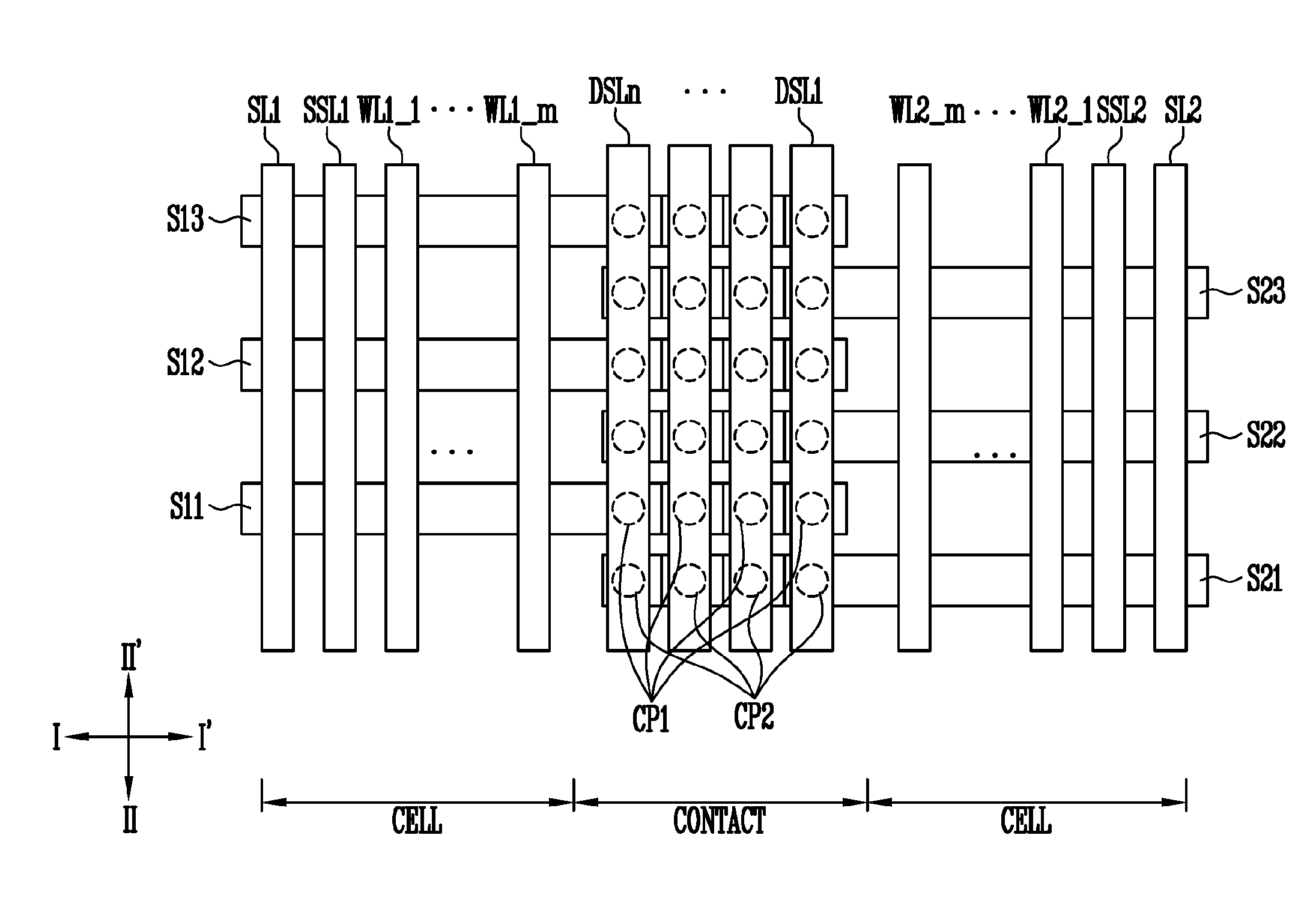
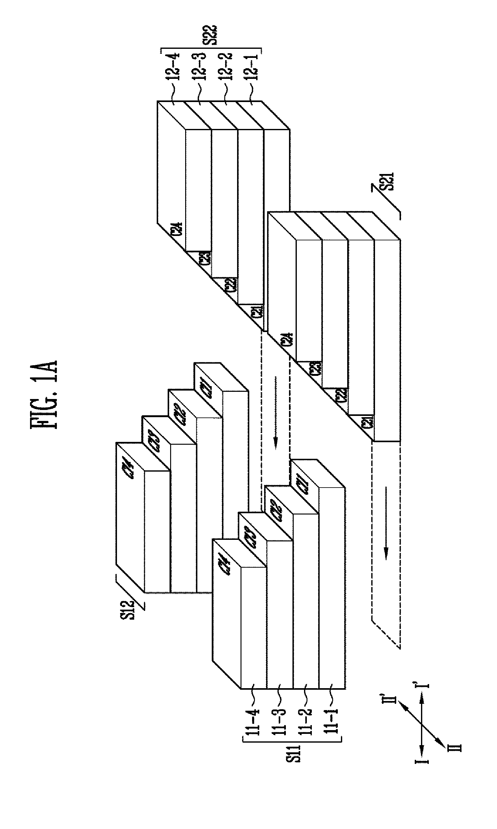
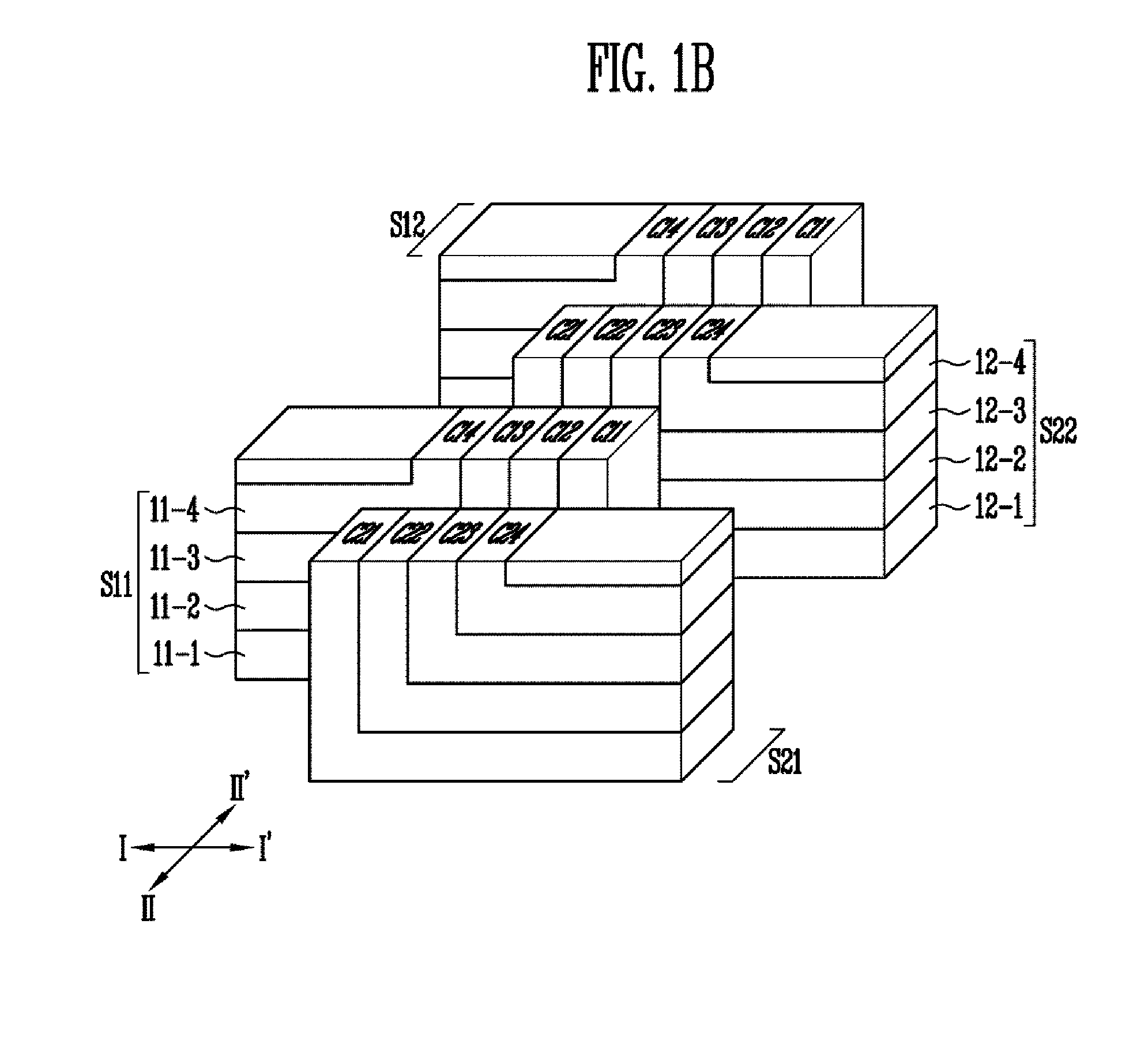
[0023]FIGS. 1A and 1B are perspective views of the structure of a semiconductor memory device according to an embodiment of the present invention. FIG. 1C is a layout view of FIGS. 1A and 1B. To facilitate understanding of the present invention, FIGS. 1A and 1B mainly illustrate a contact region, and FIG. 1C illustrates laid out layers included in a single stacked structure by laying out layers included in the single stacked ...


PUM


Abstract

A semiconductor memory device includes a plurality of first stacked structures including a plurality of first material layers at ends of which first contact regions are defined, a plurality of second stacked structures including a plurality of second material layers, wherein second contact regions are defined at ends of the second material layers and arranged between the first stacked structures so that the first contact regions and the second contact regions overlap each other, and a plurality of lines coupled in common to the first contact regions and the second contact regions.

Description

CROSS-REFERENCE TO RELATED APPLICATION[0001]The present application claims priority to Korean patent application number 10-2013-0097143 filed on Aug. 16, 2013, in the Korean Intellectual Property Office, the entire disclosure of which is incorporated by reference herein.BACKGROUND[0002]1. Technical Field[0003]Various embodiments relate generally to an electronic device and a method of operating the same and, more particularly, to a semiconductor memory device including three-dimensionally stacked memory cells.[0004]2. Related Art[0005]A non-volatile memory device preserves the stored data even when the power is cut off. Two-dimensional memory devices in which memory cells are fabricated in a single layer over a silicon substrate have reached physical limits in increasing their degree of integration. Accordingly, three-dimensional (3D) non-volatile memory devices in which memory cells are stacked in a vertical direction over a silicon substrate have been proposed.[0006]A three-dimens...

Claims


Application Information

Patent Timeline
IPC IPC(8): G11C5/02
CPCG11C5/02G11C5/025G11C5/063H01L21/76877H01L21/823487H01L27/0688H10B41/20H10B41/27H10B43/20H10B43/27
Inventor CHOI, EUN SEOK
Owner SK HYNIX INC
Why Eureka
Try Eureka