
Atomic layer deposition

a technology of atomic layer and coating, applied in the direction of coating, natural mineral layered products, chemical instruments and processes, etc., can solve the problems of delay, interruption or intervention, and achieve the effect of enhancing the deposition cycl

Inactive Publication Date: 2015-04-02
DYSON TECH LTD
View PDF2 Cites 254 Cited by
  • Summary
  • Abstract
  • Description
  • Claims
  • Application Information

AI Technical Summary

Benefits of technology

The technical effects of this patent are that the features and benefits described in the first aspect of the invention are also applicable to each of the second to sixth aspects of the invention. This allows for a more comprehensive and detailed understanding of the invention's overall benefits and capabilities.

Problems solved by technology

On the other hand, the delay occurs only after one complete atomic layer deposition and it interrupts or intervenes with continuous deposition process flow.

Method used


Image

  • Atomic layer deposition
  • Atomic layer deposition
  • Atomic layer deposition

Examples


Embodiment Construction

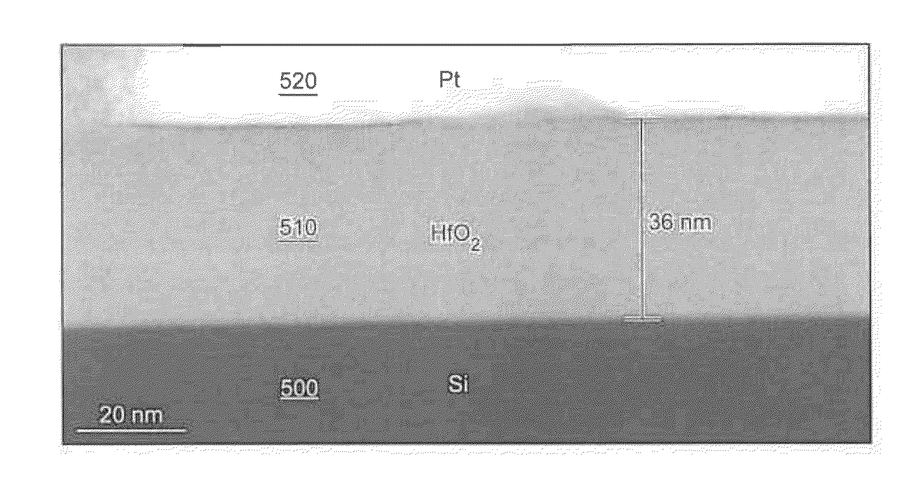
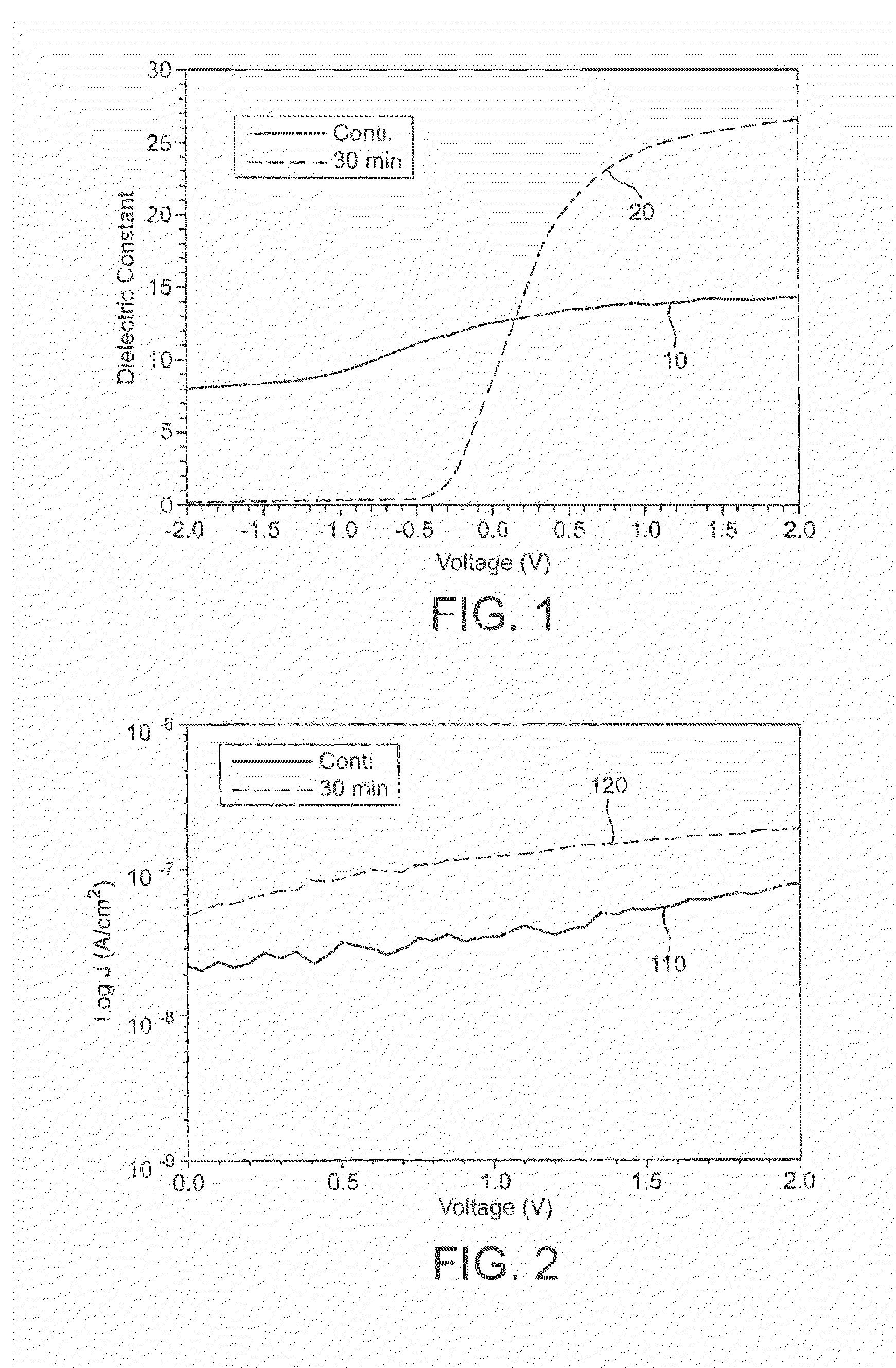
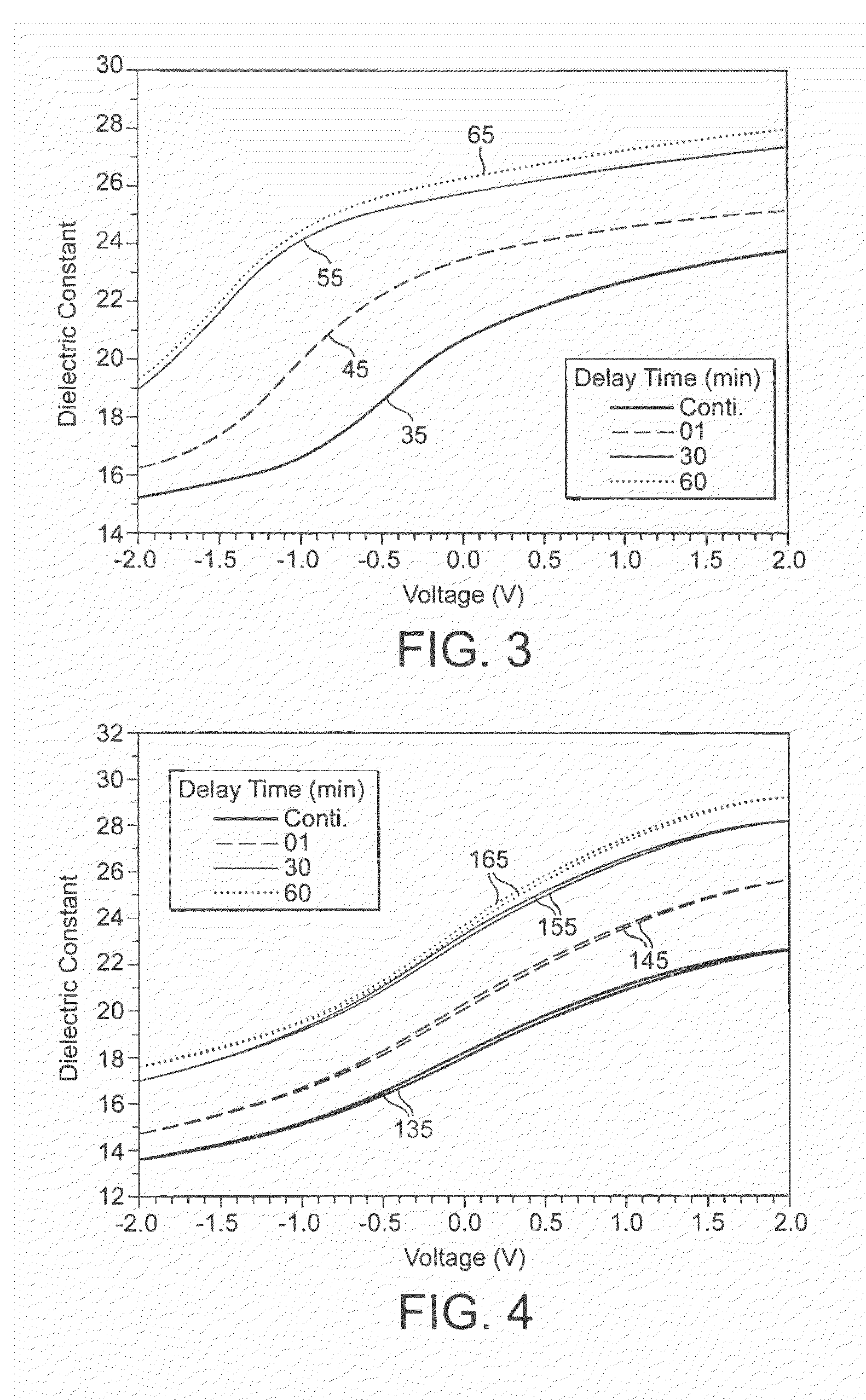
[0053]The invention utilises an atomic layer deposition process to form a thin film or coating on a substrate. The following examples describe a method for forming a coating of a dielectric material on a substrate, which may be a high-k dielectric material used in transistor and capacitor fabrication. The atomic layer deposition process comprises a plurality of deposition cycles. In this example, each deposition cycle is a plasma enhanced atomic layer deposition (PEALD) cycle, which comprises the steps of (i) introducing a precursor to a process chamber, in which a substrate is located, (ii) purging the chamber with a purge gas to remove any excess precursor from the chamber and, (iii) striking a plasma within the chamber and supplying an oxidizing precursor to the chamber to react with precursor adsorbed on the surface of the substrate to form an atomic layer on the substrate, and (iv) purging the chamber with the purge gas to remove any excess oxidizing precursor from the chamber....


PUM

PropertyMeasurementUnit
Timeaaaaaaaaaa
Dielectric polarization enthalpyaaaaaaaaaa
Pressureaaaaaaaaaa

Abstract

A method of depositing a material on a substrate using an atomic layer deposition process, wherein the deposition process comprises a first deposition step, a second deposition step subsequent to the first deposition step, and a delay of at least one minute between the first deposition step and the second deposition step. Each deposition step comprises a plurality of deposition cycles. The delay is introduced to the deposition process by prolonging a period of time for which a purge gas is supplied to a process chamber housing the substrate at the end of a selected one of the deposition cycles.

Description

REFERENCE TO RELATED APPLICATIONS[0001]This application is a national stage application under 35 USC 371 of International Application No. PCT / GB2013 / 050873, filed Apr. 3, 2013, which claims the priority of United Kingdom Application No. 1206096.8, filed Apr. 5, 2012, the entire contents of which are incorporated herein by reference.FIELD OF THE INVENTION[0002]This invention relates to a method of coating a substrate using atomic layer deposition.BACKGROUND OF THE INVENTION[0003]Atomic layer deposition (ALD) is a thin film deposition technique whereby a given amount of material is deposited during each deposition cycle. Thus it is easy to control coating thickness. One downside is the speed at which a coating is built up.[0004]ALD is based on sequential deposition of individual or fractional monolayers of a material. The surface on which the film is to be deposited is sequentially exposed to different precursors followed by purging of the growth reactor so as to remove any residual c...

Claims


Application Information

Patent Timeline
IPC IPC(8): H01L49/02H01L21/02C23C16/06C23C16/455C23C16/52
CPCH01L28/40C23C16/455C23C16/52H01L21/0228H01L21/02181H01L21/02186C23C16/06C23C16/40C23C16/45527C23C16/405C23C16/45536C23C16/45542
Inventor AMARATUNGA, GEHAN ANJIL JOSEPHCHOI, YOUNGJINSHIVAREDDY, SAI GIRIDHARBROWN, NATHAN CHARLESCOLLIS, CHARLES ANTHONY NEILD
Owner DYSON TECH LTD
Features
  • Generate Ideas
  • Intellectual Property
  • Life Sciences
  • Materials
  • Tech Scout
  • Unparalleled Data Quality
  • Higher Quality Content
  • 60% Fewer Hallucinations
Learn More