Semiconductor storing device and redundancy method thereof

a technology of storing device and semiconductor, applied in the field of redundancy of nand flash memory, can solve the problems of reducing the efficiency of compensation using redundancy data, failure to increase the yield rate of chips, and difficulty in manufacturing storing elements without flaws and defects, so as to improve the yield rate and increase the efficiency of compensation

Active Publication Date: 2015-04-30
WINBOND ELECTRONICS CORP
View PDF12 Cites 11 Cited by
  • Summary
  • Abstract
  • Description
  • Claims
  • Application Information

AI Technical Summary

Benefits of technology

[0025]According to the invention, as compared to the currently existing redundancy method, the method disclosed in the invention allows...

Problems solved by technology

As a result, it is difficult to manufacture storing elements without flaws and defects.
Therefore, when evenly allocate the redundancy bits of the redundancy storing area MR to ½ page o...

Method used


Image

  • Semiconductor storing device and redundancy method thereof
  • Semiconductor storing device and redundancy method thereof
  • Semiconductor storing device and redundancy method thereof

Examples


Embodiment Construction

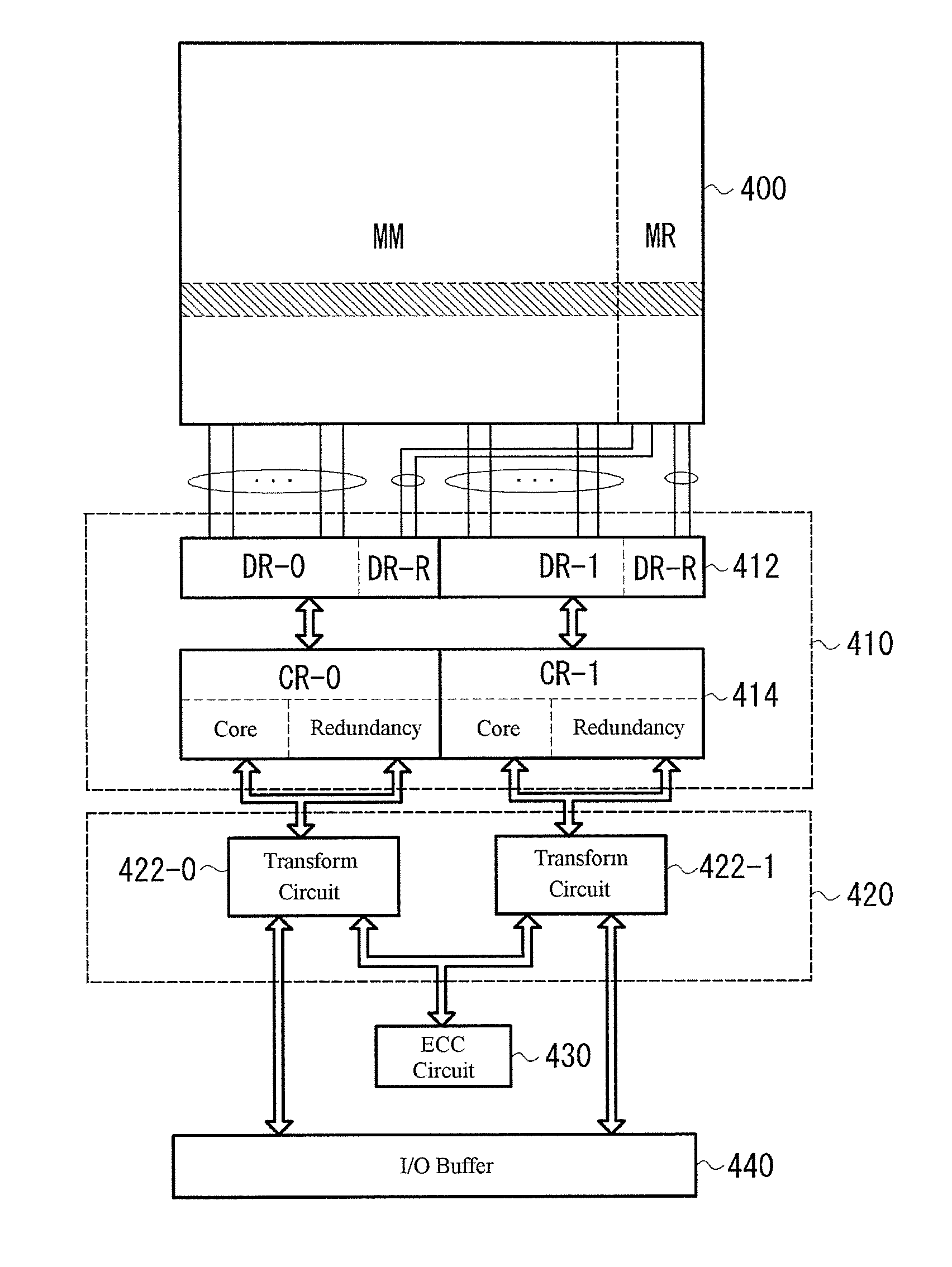
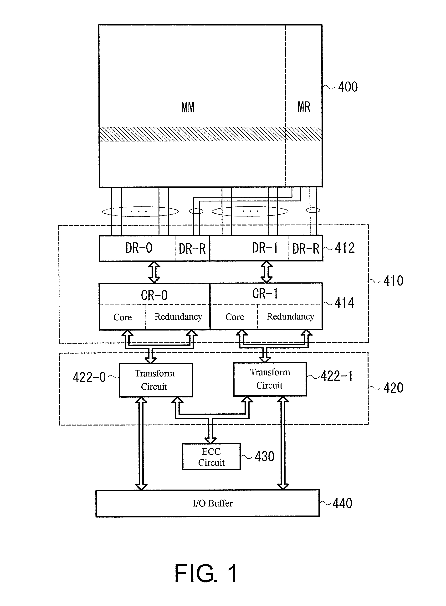
[0036]Next, the detailed descriptions accompanied by figures according to embodiments of the invention will be presented below. The invention is applicable to nonvolatile memories having various types of storing scheme. Herein, NAND flash memory is utilized as an example for a preferred embodiment. In addition, it is worth to note that parts of the accompanied figures are exaggerated to emphasize on certain features to make it more apparent for understanding, and the proportion thereof is different from the real devices.

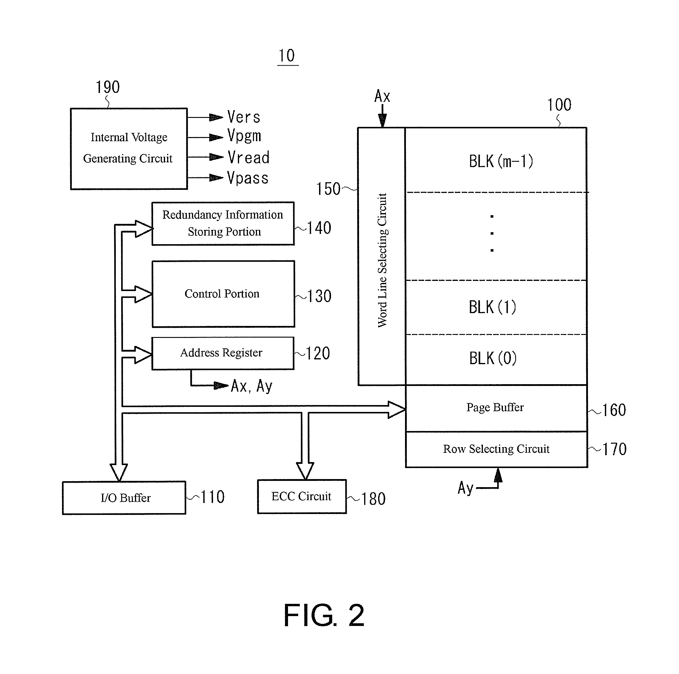
[0037]FIG. 2 is a schematic diagram illustrating typical scheme of a flash memory according to an embodiment of the invention. However, the flash memory presented herein is only an example for explanation, and the scheme of the invention is not limited herein. The flash memory 10 according to the present embodiment includes: a storing array 100, formed by a plurality of memory cells arranged in matrix; an I / O buffer 110, connected to an external I / O terminal, adapted...


PUM


Abstract

A semiconductor storing device and a redundancy method thereof are provided. The semiconductor storing device is for example a NAND flash memory, which includes: a storing array including a storing area and a redundancy storing area with a redundancy element; a page buffer; a row selecting circuit; an ECC circuit; and an I/O buffer. The row selecting circuit transforms defect data included in core data retained by a cache register into redundancy data retained by a redundancy cache register, and provides the transformed data to the ECC circuit, and the data corrected by the ECC circuit as the core data is written to the cache register again. During this period, the row selecting circuit outputs the corrected data retained in the cache register to the I/O buffer.

Description

CROSS-REFERENCE TO RELATED APPLICATION[0001]This application claims the priority benefit of Japan application serial no. 2013-220913, filed on Oct. 24, 2013. The entirety of the above-mentioned patent application is hereby incorporated by reference herein and made a part of this specification.BACKGROUND OF THE INVENTION[0002]1. Field of the Invention[0003]The invention generally relates to a semiconductor storing device, and more particularly to a redundancy of a NAND Flash Memory.[0004]2. Description of Related Art[0005]In semiconductor memories such as NAND flash memory, dynamic random access memory or the likes, the integrity thereof increases year by year. As a result, it is difficult to manufacture storing elements without flaws and defects. Therefore, a redundancy method which compensates the physical defects in appearance of the storing elements generated during manufacturing process has been adapted on a storing chip. For example, in some redundancy methods, an address conve...

Claims


Application Information

Patent Timeline
IPC IPC(8): G06F11/10
CPCG06F11/1068G06F11/1048G11C29/42G11C29/44G11C29/4401G11C2029/1208
Inventor NAKAGAWA, HARUNOBU
Owner WINBOND ELECTRONICS CORP
Why Eureka
Try Eureka