Silicon-based photoelectric integrated chip device and transmitting system with silicon-based photoelectric integrated chip device

A technology of optoelectronic integration and integrated optics, applied in circuits, electrical components, semiconductor devices, etc., can solve the problems of high price, large size of any signal shaper, and difficulty in large-scale application, so as to reduce the size of the device and improve the bandwidth compensation. Efficiency, effect of reducing manufacturing cost

Active Publication Date: 2020-06-23
NANO BEIJNANO TECH (BEIJING) CO LTDING PHOTONICS
View PDF4 Cites 4 Cited by
  • Summary
  • Abstract
  • Description
  • Claims
  • Application Information

AI Technical Summary

Problems solved by technology

Arbitrary signal shapers based on space optics and liquid crystal on silicon (LCoS) technology are bulky and expensive, making it difficult to apply them on a large scale in communications, and are often only used in experimental research fields

Method used


Image

  • Silicon-based photoelectric integrated chip device and transmitting system with silicon-based photoelectric integrated chip device
  • Silicon-based photoelectric integrated chip device and transmitting system with silicon-based photoelectric integrated chip device
  • Silicon-based photoelectric integrated chip device and transmitting system with silicon-based photoelectric integrated chip device

Examples


Embodiment Construction

[0028] Reference will now be made in detail to the exemplary embodiments, examples of which are illustrated in the accompanying drawings. When the following description refers to the accompanying drawings, the same numerals in different drawings refer to the same or similar elements unless otherwise indicated. The implementations described in the following exemplary examples do not represent all implementations consistent with the present invention. Rather, they are merely examples of systems consistent with aspects of the invention as recited in the appended claims.

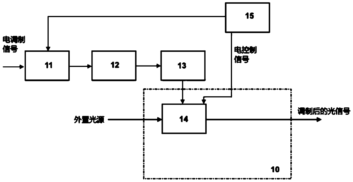
[0029] figure 1 Shown is a traditional silicon-based optoelectronic chip emission system block diagram. The electrical modulation signal is digitally pre-compensated DPC by DSP 11, then transmitted to DAC 12 to convert the digital signal into an analog signal, then amplified by the driver 13, and finally loaded on the on-chip integrated electro-optic modulator 14 to modulate the electrical signal into an optic...


PUM


Abstract

The invention discloses a silicon-based photoelectric integrated chip device and a transmitting system with the device, and the device comprises: an on-chip integrated electro-optical modulator whichis used for receiving an input light source and modulating an input electric modulation signal into an optical signal; an on-chip integrated optical filter which is used for filtering the modulated optical signal from the on-chip integrated electro-optical modulator and outputting the modulated and filtered optical signal; and at least one on-chip integrated optical coupler which is used for outputting the modulated and filtered optical signal. The on-chip integrated optical filter is adopted to roughly compensate the bandwidth of the transmitting system, and the on-chip integrated electro-optical modulator is adopted to finely compensate, so that the bandwidth compensation efficiency is improved, the signal-to-noise ratio is improved, the size of the device is reduced, and the manufacturing cost is reduced.

Description

technical field [0001] The invention relates to the field of semiconductor integrated circuit chips, in particular to a silicon-based optoelectronic integrated chip device and an emission system with the silicon-based optoelectronic integrated chip device. Background technique [0002] Silicon photonic integrated circuits (Si PICs) have gained tremendous attention due to the high-density integration capabilities of couplers, modulators, photodiodes, avalanche photodiodes, polarization diversity components, and multimode interferometers. With the increasing demand for bandwidth, the modulation rate of mainstream applications continues to increase, and the complexity of modulation formats gradually increases. However, the bandwidth of the optical transmission system is limited by the bandwidth of the modulator, the bandwidth of the driver, and the bandwidth of the package, and it is difficult to meet the increasing requirements of the modulation rate and modulation format. ...

Claims


Application Information

Patent Timeline
Patent Type & Authority Applications(China)
IPC IPC(8): H01L31/12H01L31/0232
CPCH01L31/02327H01L31/12H01L31/125
Inventor 方舟蔡鹏飞张宁
Owner NANO BEIJNANO TECH (BEIJING) CO LTDING PHOTONICS
Why Eureka
Try Eureka