
Radio frequency and microwave imaging with a two-dimensional sensor array

a sensor array and radio frequency and microwave radiation technology, applied in the field of electromagnetic wave detection, can solve the problems of time-consuming and expensive, unable to take an instantaneous image of the rf emission of the device, and unable to scan an entire electrical device with a sniffer

Active Publication Date: 2015-05-07
LENOVO ENTERPRISE SOLUTIONS SINGAPORE
View PDF5 Cites 21 Cited by
  • Summary
  • Abstract
  • Description
  • Claims
  • Application Information

AI Technical Summary

Benefits of technology

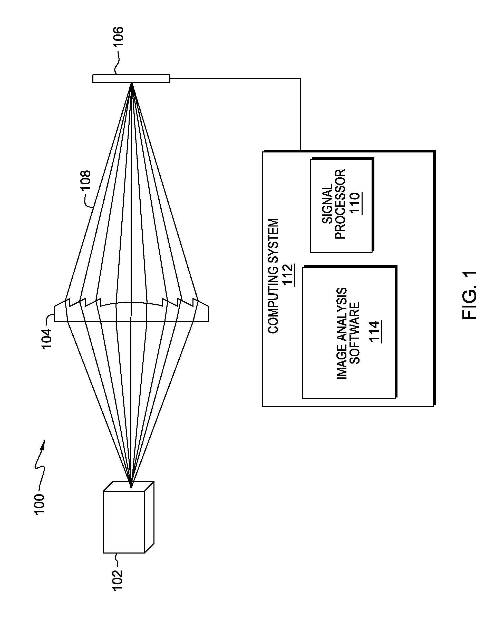
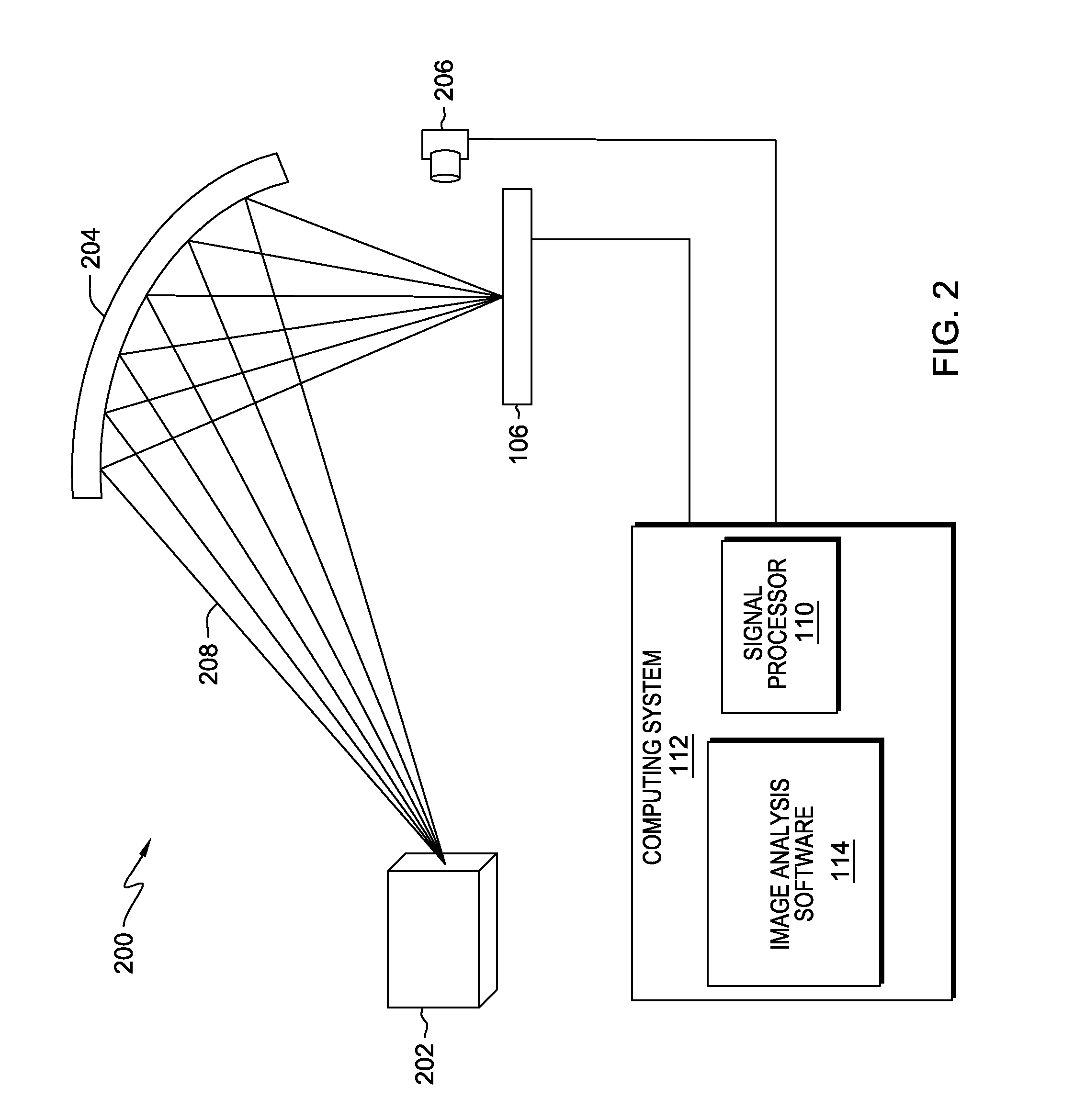
The present invention is a method, computer program product, and system for using a two-dimensional sensor array to detect and image radio and microwave electromagnetic radiation emitted from an electrical device. The sensor array is made up of multiple sensors that can detect different frequencies of radiation, which is then focused into an image using a focusing mechanism. The detected radiation is mapped to a specific location on the sensor array and converted into a computer-readable image. This technology allows for more efficient and accurate detection and imaging of electromagnetic radiation.

Problems solved by technology

Scanning an entire electrical device with a sniffer can be time consuming and expensive.
The sniffer also cannot take an instantaneous image of the RF emissions from the device.
This method can be used to generate an image of the RF emission profile of the DUT, but it is time consuming as the operator must wait for the table to move so that each point of interest on the DUT passes beneath the antenna.
A scanner is unable to produce an instantaneous image of the RF emission profile of the DUT.

Method used


Image

  • Radio frequency and microwave imaging with a two-dimensional sensor array
  • Radio frequency and microwave imaging with a two-dimensional sensor array
  • Radio frequency and microwave imaging with a two-dimensional sensor array

Examples


Embodiment Construction

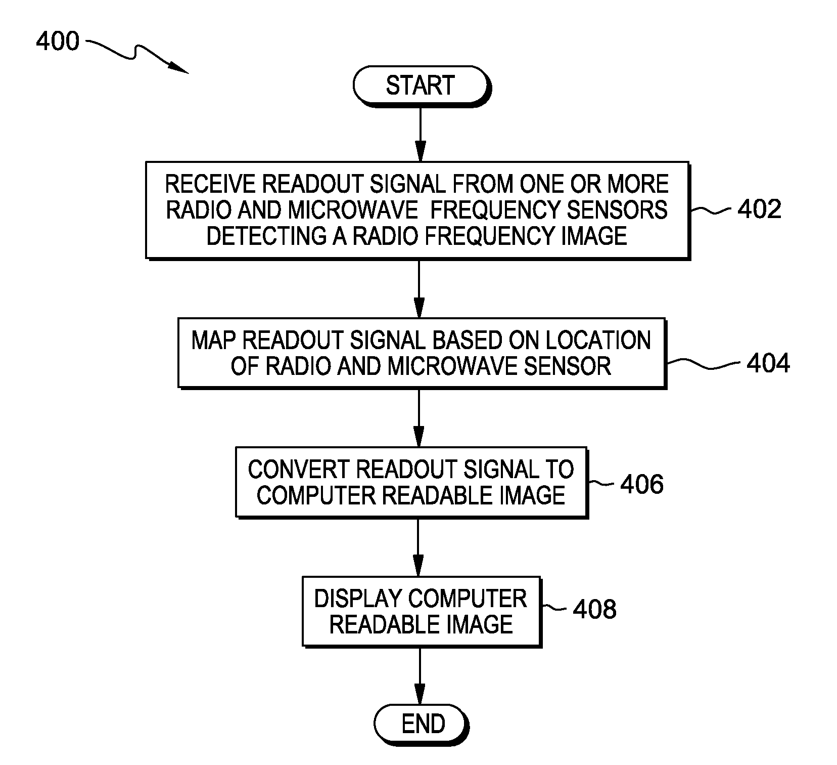
[0011]Embodiments of the present invention recognize that limiting the RF emission from electrical devices is an important part of designing enclosures for the electrical devices. RF emissions are governmentally regulated and can interfere with electronics outside of the enclosure if RF leaks are not eliminated from the device. Therefore, efficient and effective methods of detecting RF emissions from an electronic device are necessary to prevent electrical interference between devices. RF radiation can be detected using an RF antenna attached to an oscilloscope or a spectral analyzer. Embodiments of the present invention include an RF focusing device and an array of RF antennas that can be used to take an RF snapshot of the device, similar to a photograph. The RF snapshot can then be compared to the device to determine the location of potential RF radiation leaks from the device enclosure.

[0012]The present invention will now be described in detail with reference to the Figures. FIG....


PUM


Abstract

Embodiments of the present invention disclose a method, computer program product, and system for imaging radio and microwave electromagnetic radiation using a two-dimensional sensor array. A computing system receives a readout signal from one or more of a plurality of frequency sensors, arranged in a two-dimensional array, that have the ability to detect an image of focused radio and microwave frequency radiation. The computing system maps the readout signal of each of the plurality of sensors to a location corresponding to the physical location of the sensor on the two-dimensional array. The computing system converts the readout signal into a computer readable image.

Description

FIELD OF THE INVENTION[0001]This disclosure relates generally to electromagnetic wave detection and more specifically to detecting radio frequency and microwave radiation by imaging the source with a two-dimensional sensor array.BACKGROUND OF THE INVENTION[0002]Manufactured electronic products may have limits on the amount of electromagnetic radiation that they are allowed to emit. For example, governmental regulations define maximal electromagnetic radiation emission limitations. Part of these limitations are focused on the radio frequency and microwave (hereinafter RF) portion of the electromagnetic spectrum. Therefore, one part of product design includes ensuring that the electronic circuitry has minimal RF emission and that the emissions are confined inside of an enclosure. Ensuring that emissions are confined inside of an enclosure involves detecting possible leakages, or gaps, in the enclosure from which RF radiation can escape.[0003]Current techniques for detecting such gaps ...

Claims


Application Information

Patent Timeline
Patent Type & Authority Applications(United States)
IPC IPC(8): G01R31/00
CPCG01R31/001G01R29/0814
Inventor AO, ERIC R.
Owner LENOVO ENTERPRISE SOLUTIONS SINGAPORE
Learn More