Fingerprint recognition sensor module having sensing region separated from asic
a fingerprint recognition and sensor module technology, applied in the field of fingerprint recognition sensor modules, can solve the problems of personal information and content recorded and stored in mobile devices that are often leaked without user intent, security problems and limitations in mobile device design, etc., to enhance contact performance, enhance sensing sensitivity, and increase sensing sensitivity
- Summary
- Abstract
- Description
- Claims
- Application Information
AI Technical Summary
Benefits of technology
Problems solved by technology
Method used
Image

Examples
first embodiment
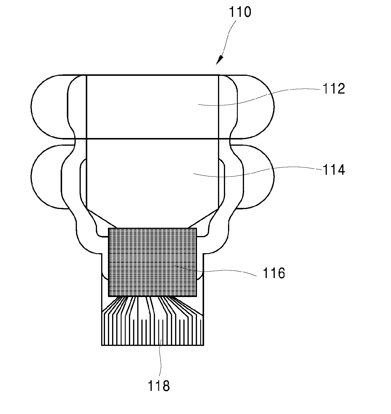
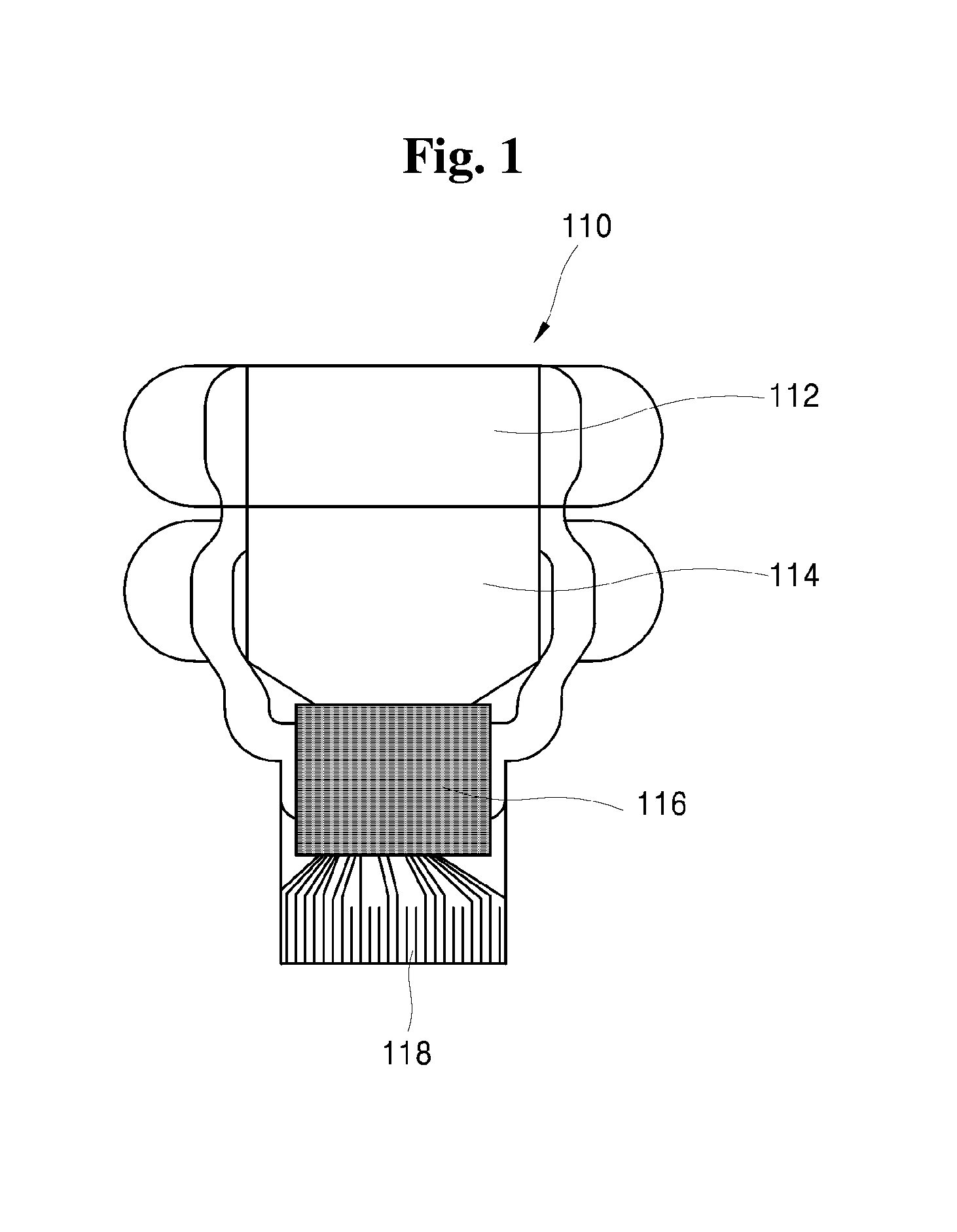
[0056]FIG. 1 is a plan view of a flexible printed circuit board for fabrication of a fingerprint recognition sensor module according to the invention.
[0057]Referring to FIG. 1, a flexible printed circuit board 110 for fabrication of a fingerprint recognition sensor module according to the first embodiment of the invention includes a first sensing region 112 formed with a first sensing input unit, a second sensing region 114 formed with a second sensing input unit, a chip mounting region 116 on which an ASIC operated in response to signals sensed through the sensing input units is mounted, and a connection section 118 to which a connector for connection to a device is attached.
[0058]The first and second sensing input units are functionally separated from each other. One of the first and second sensing input units may be a transmitter and the other may be a receiver.
[0059]A continuous current flow in the transmitter induces a uniform magnetic field. Here, when the transmitter is touch...
second embodiment
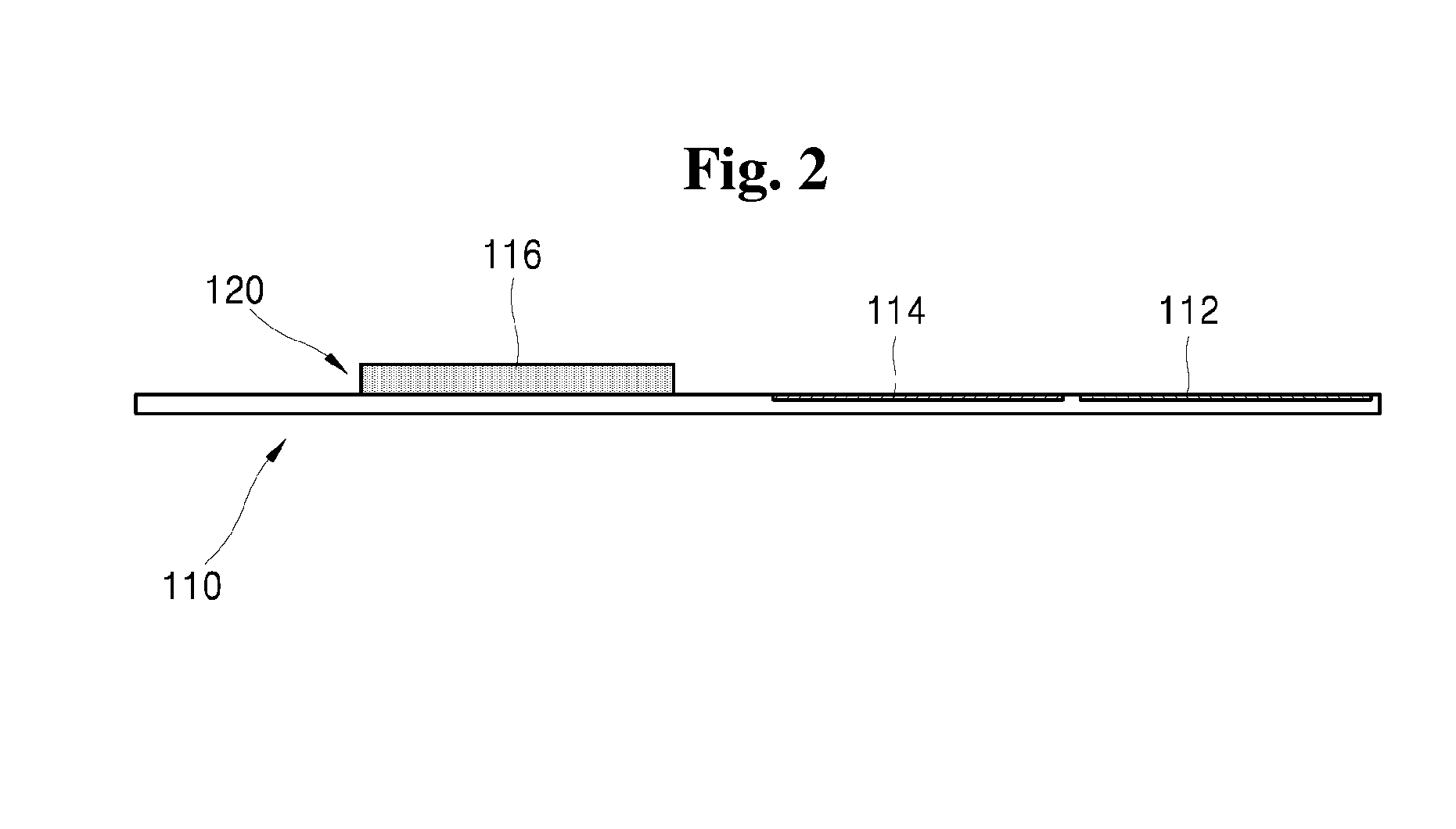
[0066]FIG. 4 is a side view of a flexible printed circuit board for fabrication of a fingerprint recognition sensor module according to the invention.
[0067]The second embodiment is the same as the first embodiment in that first and second sensing regions 112, 114 and a chip mounting region 116 are formed to be separated from each other. However, in the first embodiment, the first and second sensing regions 112, 114 and the chip mounting region 116 are formed on the same surface, whereas in the second embodiment, the first and second sensing regions 112, 114 are formed on the same surface and the chip mounting region 116 is formed on a surface opposite to the surface on which the sensing regions 112, 114 are formed.
[0068]As in the first embodiment, the first and second sensing regions 112, 114 and the chip mounting region 116 are also superposed one above another in the finished fingerprint recognition sensor module according to the second embodiment, and thus repetitive descriptions...
third embodiment
[0069]FIG. 5 is a side view of a flexible printed circuit board for fabrication of a fingerprint recognition sensor module according to the invention.
[0070]The third embodiment is the same as the aforementioned embodiments in that first and second sensing regions 112, 114 and a chip mounting region 116 are formed to be separated from each other. However, in the third embodiment, the first and second sensing regions 112, 114 are formed on different surfaces.
[0071]Although the chip mounting region 116 and the first sensing region 112 are formed on the same surface in FIG. 5, the chip mounting region 116 and the second sensing region 114 may also be formed on the same surface.
[0072]As in the aforementioned embodiments, the first and second sensing regions 112, 114 and the chip mounting region 116 are also superposed one above another in the finished fingerprint recognition sensor module according to the third embodiment.
[0073]FIG. 6 is a side view of a flexible printed circuit board fo...
PUM
| Property | Measurement | Unit |
|---|---|---|
| Thickness | aaaaa | aaaaa |
| Thickness | aaaaa | aaaaa |
| Dielectric polarization enthalpy | aaaaa | aaaaa |
Abstract
Description
Claims
Application Information
 - R&D Engineer
- R&D Manager
- IP Professional
- Industry Leading Data Capabilities
- Powerful AI technology
- Patent DNA Extraction
Browse by: Latest US Patents, China's latest patents, Technical Efficacy Thesaurus, Application Domain, Technology Topic.
© 2024 PatSnap. All rights reserved.Legal|Privacy policy|Modern Slavery Act Transparency Statement|Sitemap