Lens array and method of making same

Inactive Publication Date: 2005-09-06
TANG YIN S
View PDF8 Cites 29 Cited by
  • Summary
  • Abstract
  • Description
  • Claims
  • Application Information

AI Technical Summary

Benefits of technology

[0014]In other embodiments, the dielectric layer can be deposited over any substrate and does not have to be a sensor array. In such embodiments, the process forms and/or can be used to make plastic molding templates to form individual spherical or non-spherical lenses, or an array of spherical and/or non-spherical microlenses of any desired shape or shapes. The process of the present invention allows a lens or microlens array to be formed with different shaped non-spherical and/or spherical lenses. This gives the lens manufacturer more flexibility to fabricate many additional types of lens arrays at discount prices.
[0015]The present invention provides numerous advantages over conventional microlens arrays and methods. Since the microlens array is formed directly onto the sensor array with fewer processing steps than conventional methods, microlens/sensor devices of the present invention are easier and less expensive to fabricate than conventional devices. The focal length of the microlenses can be controlled depending on the type of dielectric materials used for the microlenses and/or process control (i.e., curvature of the lens elements.)
[0016]The present invention also provides improved senso

Problems solved by technology

This color distortion increases with time due to oxidation of the resin.
Another disadvantage is that the resolution with which the photosensitive resin can be patterned is limited by the thickness of the resin layer.
The thicker the resin layer, the farther apart the microlenses in the array, which reduces the light collection efficiency of the array.
Consequently, it is difficult to obtain the highest possible collection efficiency with microlens arrays fabricated in this manner.
Yet another disadvantage results from the fact that as the curvature radius of the microlens becomes small, the incident light is focused on a point near the microlens.
Moreover, because a microlens formed in a rectangular shape has a significant difference between its curvature radius in the width and the length directions, it is difficult to focus incident light on the corresponding photodiod

Method used


Image

  • Lens array and method of making same
  • Lens array and method of making same
  • Lens array and method of making same

Examples


Embodiment Construction

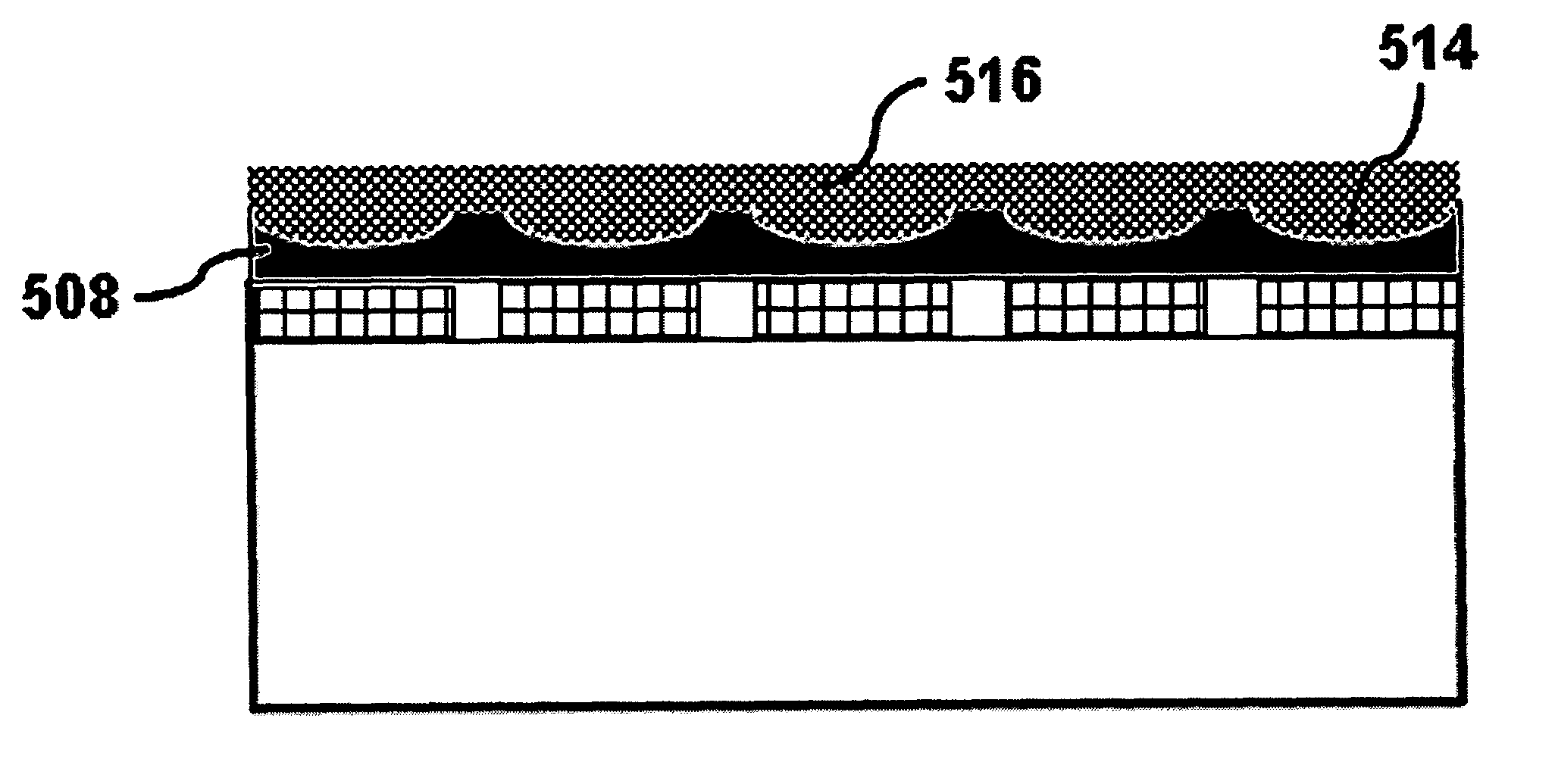
[0029]FIG. 4 is a flowchart illustrating a method 400 in accordance with an embodiment of the present invention for fabricating a microlens array or a non-spherical lens. A substrate is first provided in step 402, where the substrate may include an array of CMOS or CCD sensors. The sensor array may be any suitable size, ranging from small screen applications to large display devices. A dielectric layer is then deposited on the substrate in step 404. A patterning layer, such as a spin-on photoresist or other photosensitive material, is deposited on the dielectric layer in step 406. Selected portions of the patterning layer are removed, such as by conventional photolithography processing, in step 408. The removed portions expose areas of the dielectric layer where the microlenses or non-spherical lenses are to be formed. With embodiments having a sensor array, the exposed areas correspond to locations of individual sensor elements.

[0030]In step 410, the exposed portions of the dielect...


PUM


Abstract

Systems and methods are provided for a lens or microlens array or non-spherical lens with or without an integrated sensor unit. A dielectric between a substrate and a lens material has curved recesses, which are filled in by the lens material. Light enters the lens material layer and is focused by the curved recess portions.

Description

BACKGROUND[0001]1. Field of the Invention[0002]The present invention relates generally to microlens arrays and optical lenses, and more particularly to methods for manufacturing microlens arrays or non-spherical lenses.[0003]2. Related Art[0004]Microlens arrays provide optical versatility in a miniature package for imaging applications. Traditionally, a microlens is defined as a lens with a diameter less than one millimeter; however, a lens having a diameter as large as five millimeters or more has sometimes also been considered a microlens.[0005]There are many conventional methods for manufacturing microlens arrays, such as using reflow or diffusion. FIGS. 1A–1C show a typical sequence of steps for making a microlens array by depositing material, patterning, and reflowing. In FIG. 1A, a photosensitive layer 10, such as a photosensitive resin, is formed on a planarization layer 12 over a silicon substrate (not shown). The material of the photosensitive layer is used to form the micr...

Claims


Application Information

Patent Timeline
IPC IPC(8): G02B3/00
CPCG02B3/0012H01L27/14627G02B3/0031G02B3/0056G02B3/0043G02B3/00
Inventor TANG, YIN S.
Owner TANG YIN S
Why Eureka
Try Eureka