Lens array and method of making same

a microlens array and optical lens technology, applied in the field of microlens arrays and optical lenses, can solve the problems of reducing the light collection efficiency of the array, reducing the resolution with which the photosensitive resin can be patterned, and increasing the color distortion with time, so as to improve the reliability or useful life of the microlens, improve the sensor sensitivity, and be easy to fabricate and less expensive

Inactive Publication Date: 2005-09-15
TANG YIN S
View PDF8 Cites 21 Cited by
  • Summary
  • Abstract
  • Description
  • Claims
  • Application Information

AI Technical Summary

Benefits of technology

[0014] In other embodiments, the dielectric layer can be deposited over any substrate and does not have to be a sensor array. In such embodiments, the process forms and / or can be used to make plastic molding templates to form individual spherical or non-spherical lenses, or an array of spherical and / or non-spherical microlenses of any desired shape or shapes. The process of the present invention allows a lens or microlens array to be formed with different shaped non-spherical and / or spherical lenses. This gives the lens manufacturer more flexibility to fabricate many additional types of lens arrays at discount prices.
[0015] The present invention provides numerous advantages over conventional microlens arrays and methods. Since the microlens array is formed directly onto the sensor array with fewer processing steps than conventional methods, microlens / sensor devices of the present invention are easier and less expensive to fabricate than conventional devices. The focal length of the microlenses can be controlled depending on the type of dielectric materials used for the microlenses and / or process control (i.e., curvature of the lens elements.)
[0016] The present invention also provides improved sensor sensitivity due to the ability to make non-spherical lenses using wet etching, grey-scale mask or shadow mask processing. Another advantage is that using non-organic lens materials extends the reliability or useful lifetime of the microlens. The color quality of the image produced by the sensor is also improved because the lens material does not have the adverse characteristics of resin-containing materials, which as discussed above, can absorb proportionally more blue light to make the image yellowier than desired. Yet another advantage the current invention provides is that the resulting microlens / sensor device is thinner and more resistant to environmental effects because the microlens array acts as a protection layer for the sensor elements.
[0017] The resulting microlens array may be used with devices for a variety of application, from a small display screen for a camera, a digital camera sensor, a personal digital assistant, or a laptop to a large display screen for a projection screen, a wall-sized display screen, or a billboard-sized display screen. The processing or fabrication of the array / sensor unit allows high throughput with consistent characteristics between each array / sensor unit.

Problems solved by technology

This color distortion increases with time due to oxidation of the resin.
Another disadvantage is that the resolution with which the photosensitive resin can be patterned is limited by the thickness of the resin layer.
The thicker the resin layer, the farther apart the microlenses in the array, which reduces the light collection efficiency of the array.
Consequently, it is difficult to obtain the highest possible collection efficiency with microlens arrays fabricated in this manner.
Yet another disadvantage results from the fact that as the curvature radius of the microlens becomes small, the incident light is focused on a point near the microlens.
Moreover, because a microlens formed in a rectangular shape has a significant difference between its curvature radius in the width and the length directions, it is difficult to focus incident light on the corresponding photodiode without error, and a part of the light is focused on the planarization layer or color filter layer between the photodiode and the microlens, causing loss of light and deterioration of sensitivity and resolution.
One disadvantage to forming microlens arrays using diffusion is that control of the thickness along the optical axis is limited.
Several processing steps are needed to form the separate microlens layer 32, filter layer 40, and sensor layer 42, which increase cost and time.
The layers also increase the separation between the microlenses and the sensors, which can increase crosstalk between pixels, due in part to light impinging on adjacent sensors instead of the desired sensor.
However, the fabrication of non-spherical lenses is complicated and can only be done through skilled manual operation by highly trained professionals.
This can be time consuming and costly.

Method used


Image

  • Lens array and method of making same
  • Lens array and method of making same
  • Lens array and method of making same

Examples


Embodiment Construction

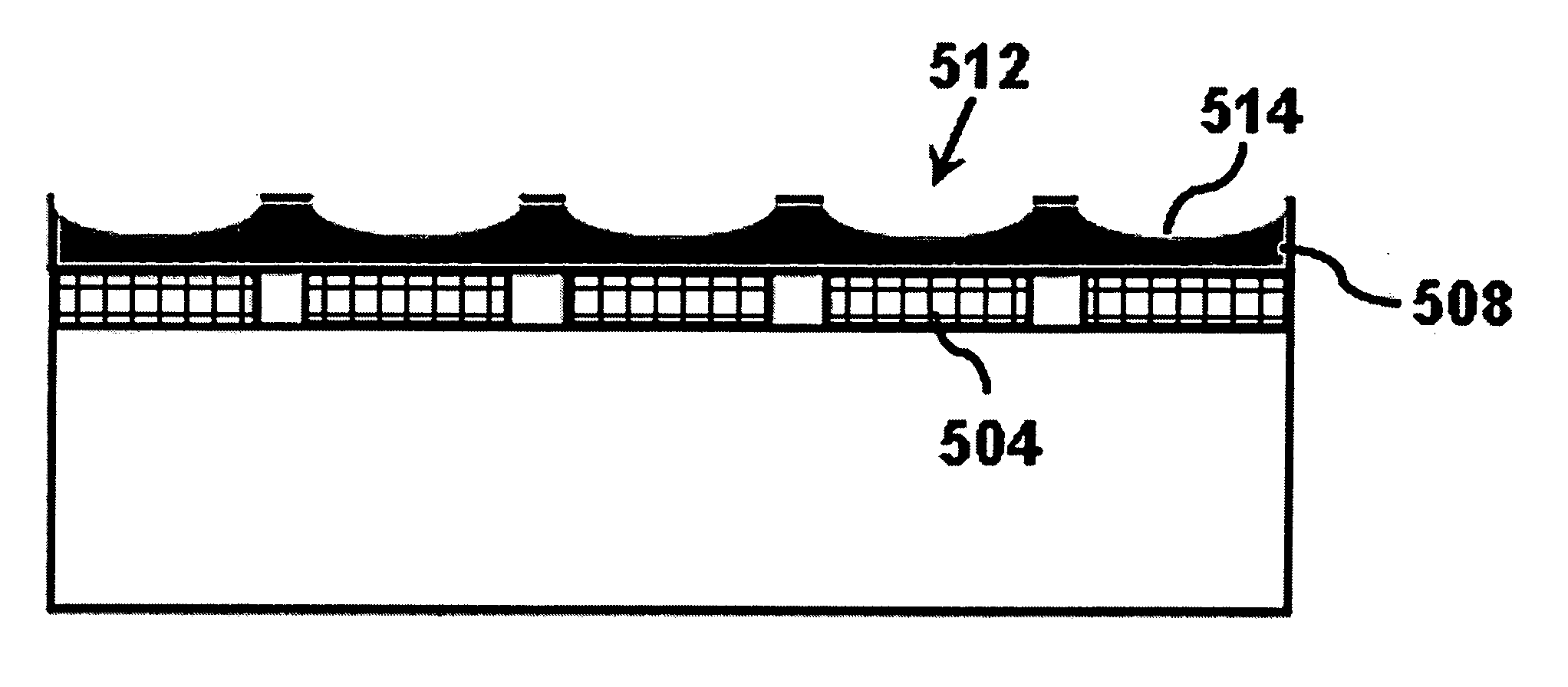
[0029]FIG. 4 is a flowchart illustrating a method 400 in accordance with an embodiment of the present invention for fabricating a microlens array or a non-spherical lens. A substrate is first provided in step 402, where the substrate may include an array of CMOS or CCD sensors. The sensor array may be any suitable size, ranging from small screen applications to large display devices. A dielectric layer is then deposited on the substrate in step 404. A patterning layer, such as a spin-on photoresist or other photosensitive material, is deposited on the dielectric layer in step 406. Selected portions of the patterning layer are removed, such as by conventional photolithography processing, in step 408. The removed portions expose areas of the dielectric layer where the microlenses or non-spherical lenses are to be formed. With embodiments having a sensor array, the exposed areas correspond to locations of individual sensor elements.

[0030] In step 410, the exposed portions of the diele...


PUM


Abstract

Systems and methods are provided for a lens or microlens array or non-spherical lens with or without an integrated sensor unit. A dielectric between a substrate and a lens material has curved recesses, which are filled in by the lens material. Light enters the lens material layer and is focused by the curved recess portions.

Description

BACKGROUND [0001] 1. Field of the Invention [0002] The present invention relates generally to microlens arrays and optical lenses, and more particularly to methods for manufacturing microlens arrays or non-spherical lenses. [0003] 2. Related Art [0004] Microlens arrays provide optical versatility in a miniature package for imaging applications. Traditionally, a microlens is defined as a lens with a diameter less than one millimeter; however, a lens having a diameter as large as five millimeters or more has sometimes also been considered a microlens. [0005] There are many conventional methods for manufacturing microlens arrays, such as using reflow or diffusion. FIGS. 1A-1C show a typical sequence of steps for making a microlens array by depositing material, patterning, and reflowing. In FIG. 1A, a photosensitive layer 10, such as a photosensitive resin, is formed on a planarization layer 12 over a silicon substrate (not shown). The material of the photosensitive layer is used to for...

Claims


Application Information

Patent Timeline
Patent Type & Authority Applications(United States)
IPC IPC(8): G02B3/00
CPCG02B3/0012G02B3/0031H01L27/14627G02B3/0056G02B3/0043G02B3/00
Inventor TANG, YIN S.
Owner TANG YIN S
Why Eureka
Try Eureka