Substrate for Preventing Burr Generation

a technology of burrs and substrates, applied in the direction of instruments, other domestic objects, transportation and packaging, etc., can solve problems such as electrical shorts, and achieve the effect of preventing electrical shorts

Active Publication Date: 2015-05-21
POINT ENG
View PDF1 Cites 0 Cited by
  • Summary
  • Abstract
  • Description
  • Claims
  • Application Information

AI Technical Summary

Benefits of technology

[0008]A substrate for an optical device is configured for preventing electrical shorts among the elements in the substrate occurring due to the burrs generated during the cutting process of the substrate for the optical device.

Problems solved by technology

However, according to the conventional methods, when a substrate for an optical device made by alternately stacking conductive plates and insulating films (or insulating layers) is being sawed or diced, burrs are generated during the dicing process, and there has been a problem in that electrical shorts are being occurred since the burrs generated due to the difference in the material hardness between the conductive plate and the insulating film are penetrating into the conductive plate by crossing the insulating film along the direction of cutting.

Method used


Image

  • Substrate for Preventing Burr Generation
  • Substrate for Preventing Burr Generation
  • Substrate for Preventing Burr Generation

Examples


Embodiment Construction

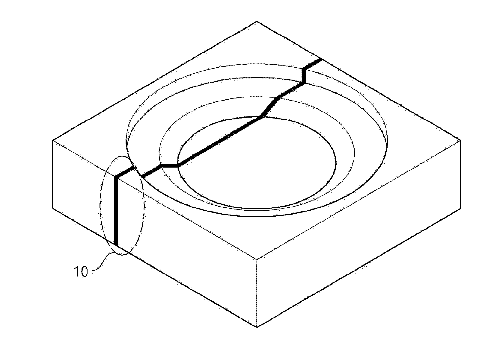
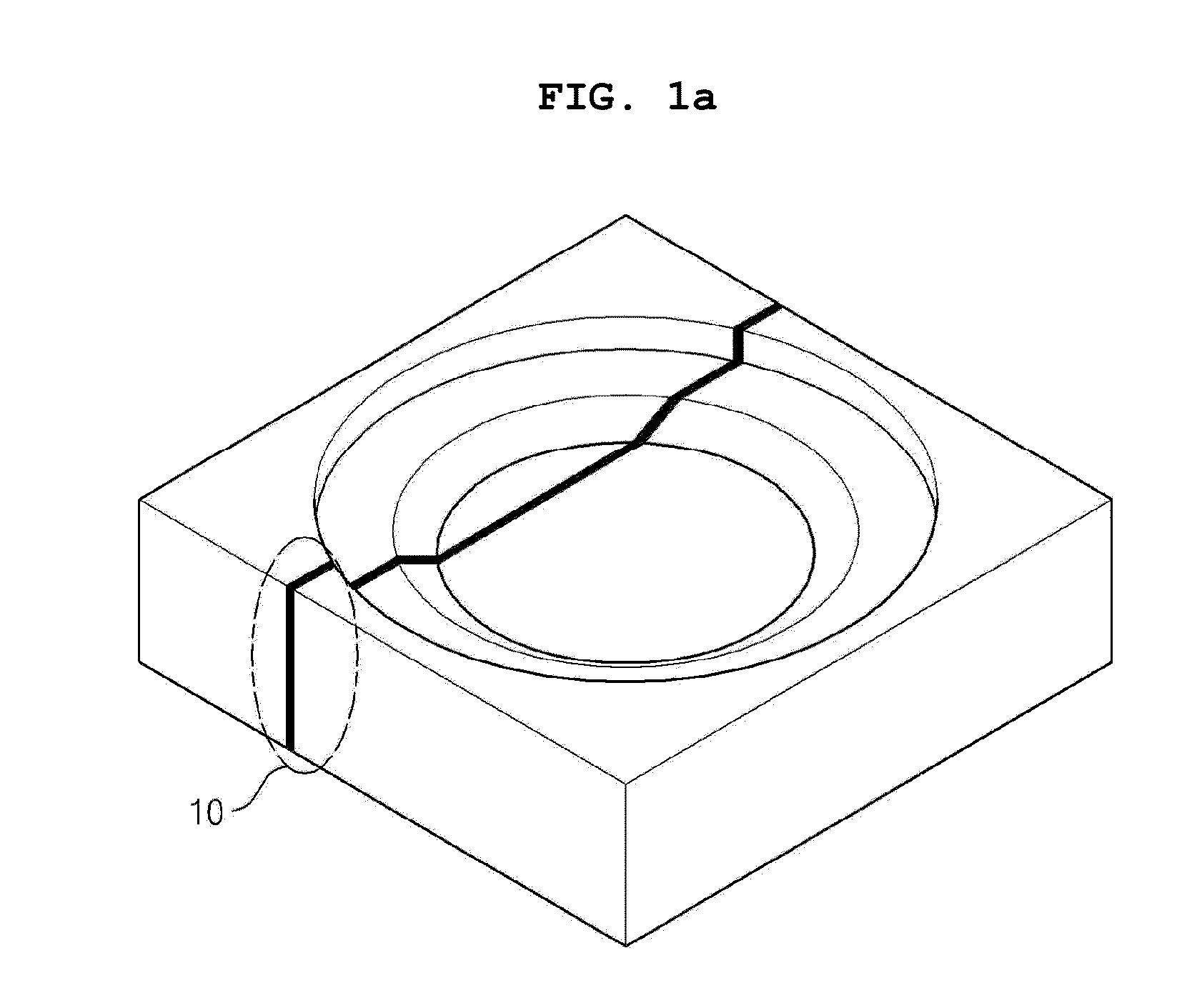
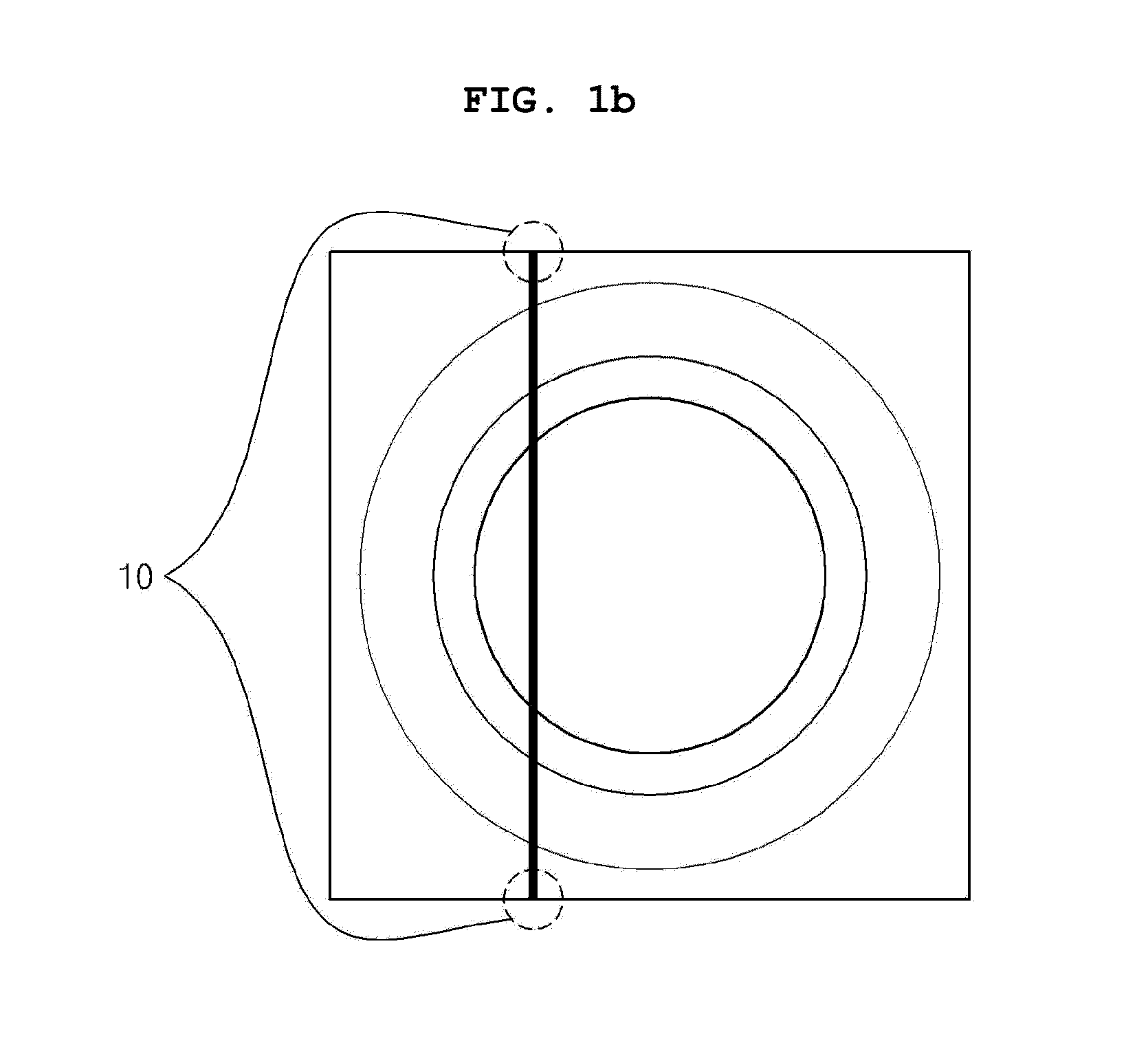
[0024]FIGS. 1a, 1b, and 1c are the exemplary drawings showing the problem of burr generation which is to be solved. FIG. 1a is a perspective view showing a chip substrate formed resulting from the cutting of a substrate for an optical device.

[0025]In the exemplary embodiment, a substrate for an optical device is an array of a plurality of chip substrates having a predetermined size, and being utilized by cutting thereof into each individual chip substrates. At this time, the cross-section 10 is formed to have a top view as shown in FIG. 1b, a side view as shown in FIG. 1c, and a bottomview as shown in FIG. 1d. When cutting a substrate in accordance with the above described drawings, burrs are generated during sawing or dicing, and the insulator, which is a very thin layer, will be damaged resulting in an insulation breakdown, therefore there is a problem of failure occurrence such as an electrical short.

[0026]A structure for a substrate for an optical device is proposed for solving ...


PUM

PropertyMeasurementUnit
lengthaaaaaaaaaa
liquid insulationaaaaaaaaaa
areaaaaaaaaaaa

Abstract

A substrate for an optical device includes an optical device substrate including a plurality of conductive plates elongated along a length direction, wherein side surfaces of the conductive plates are bonded to each other with insulators interposed therebetween, the insulators being respectively formed on the side surfaces. A groove having a predetermined depth for preventing burrs is formed in a lower surface of the optical device substrate at each point where a cutting line is crossed with one of the insulators when the optical device substrate is cut in a length direction and in a vertical direction, the groove being formed in such a way that said one of the insulators is exposed to an inside of the groove.

Description

BACKGROUND[0001]Priority is claimed from Korean Patent Application No.10-2013-0141255, the full disclosure of which is hereby incorporated by reference herein.[0002]1. Technical Field[0003]The present invention relates to a substrate for an optical device, more particularly to a substrate for an optical device for preventing electrical shorts among the elements in the substrate due to the burrs generated during the substrate cutting process.[0004]2. Description of the Related Art[0005]LEDs are being used as the light source of a back light unit (BLU) for a liquid crystal display (LCD) which is used in the flat panel displays such as TVs, computer monitors, and the like.[0006]An optical device chip such as an LED is being mounted on the substrate for an optical device, and the individual optical devices are manufactured through a separation process i.e. sawing or dicing of the substrate for the optical devices.[0007]However, according to the conventional methods, when a substrate for...

Claims


Application Information

Patent Timeline
Patent Type & Authority Applications(United States)
IPC IPC(8): G02B5/08B32B3/26
CPCG02B5/085B32B2551/00B32B3/263B32B3/26B32B2307/202B32B2307/206Y10T428/24612H01L33/00H01L33/48
Inventor AHN, BUM MONAM, KI MYUNGYOO, KYUNG SOO
Owner POINT ENG
Why Eureka
Try Eureka