Electrode structure for semiconductor chip with crack suppressing dummy metal patterns

a technology of dummy metal patterns and electrode structures, which is applied in the direction of semiconductor devices, semiconductor/solid-state device details, electrical apparatus, etc., can solve the problems of electrical shorts that occur between, and achieve the effect of suppressing crack expansion and enhancing the reliability of bump connection of electrode pads

Active Publication Date: 2012-01-03
PANASONIC SEMICON SOLUTIONS CO LTD
View PDF9 Cites 5 Cited by
  • Summary
  • Abstract
  • Description
  • Claims
  • Application Information

AI Technical Summary

Benefits of technology

[0014]Therefore, an object of the present invention is to provide an electrode structure for a semiconductor chip for preventing electrical short from occurring between solder bumps of bump electrodes adjacent to each other, and suppressing expansion of a crack generated due to bump stress concentrated on an under-edge portion below a barrier metal, so as to enhance the reliability of the bump connection of the electrode pad.
[0025]Further, preferably, the metal pattern includes a pattern for preventing expansion of a generated crack.
[0029]As described above, the electrode structure for the semiconductor chip according to the present invention enables prevention of electrical short between the solder bumps of the bump electrodes adjacent to each other, suppression of expansion of a crack generated due to bump stress concentrated on the under-edge position below the barrier metal, and enhancement of the reliability of the bump connection of the electrode pad. Further, in the electrode structure for the semiconductor chip according to the present invention, generation of a crack due to bump stress concentrated on the under-edge position of the barrier metal may not be easily caused, thereby also exerting an effect of suppressing generation of a crack.
[0030]The semiconductor device to which the electrode structure for the semiconductor chip according to the present invention is applied enables suppression of expansion of a crack generated due to bump stress, and enhancement of the reliability of connection of the solder bump, so that the diameter of the bump can be reduced for the flip-chip connection so as to reduce a pad pitch, and therefore the present invention is applicable for increasing a density of the semiconductor device, or the like.

Problems solved by technology

However, the structure of the conventional bump electrode 1300 shown in FIG. 13 causes a problem that malfunction that an electrical short often occurs between the solder bumps of the bump electrodes adjacent to each other when plating, which is a typical technique for forming a solder bump, is performed. FIG. 14 is a diagram illustrating a state where the electrical short occurs between the solder bumps 1103 of the bump electrodes 1300, shown in FIG. 13, adjacent to each other.

Method used


Image

  • Electrode structure for semiconductor chip with crack suppressing dummy metal patterns
  • Electrode structure for semiconductor chip with crack suppressing dummy metal patterns
  • Electrode structure for semiconductor chip with crack suppressing dummy metal patterns

Examples


first embodiment

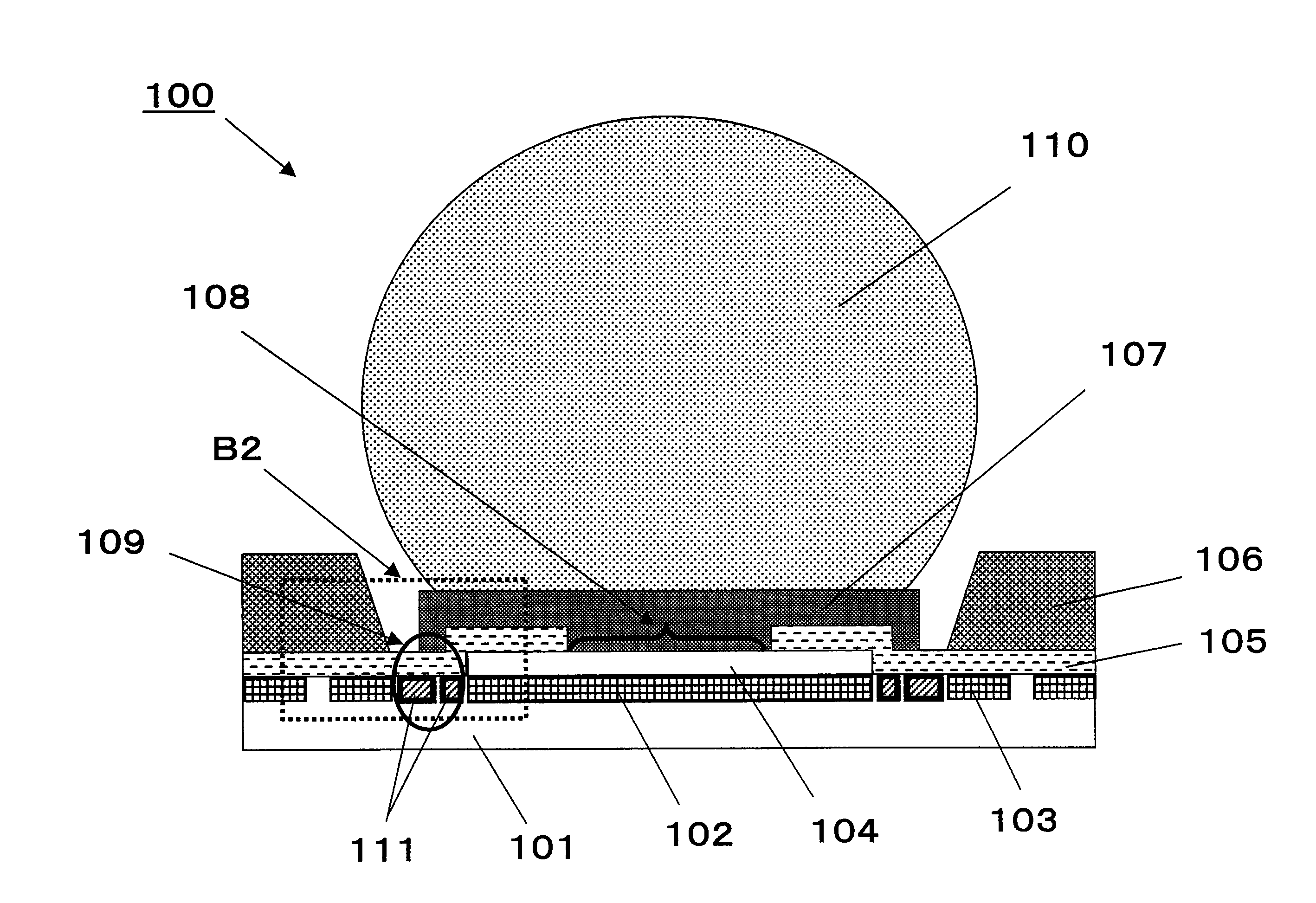
[0054]FIG. 1 is a diagram illustrating a bump electrode 100 for a semiconductor device according to a first embodiment of the present invention. In FIG. 1, the bump electrode 100 has a structure in which a pad-form wiring metal 102 and a wiring metal 103 are positioned in the uppermost layer portion of a silicon 101. A pad connecting metal 104 is positioned on the pad-form wiring metal 102. The upper surfaces of the silicon 101 and the pad connecting metal 104 are covered by a nitride protective film 105 mainly formed by a nitride film so as to protect the pad connecting metal 104. However, a part of the upper surface of the pad connecting metal 104 forms an opening 108 which is not covered by the nitride protective film 105. The pad connecting metal 104 contacts a barrier metal 107 at the opening 108, and therefore the pad connecting metal 104 electrically connects to a solder bump 110 formed on the barrier metal 107. A resin material protective film 106 is provided on the nitride ...

second embodiment

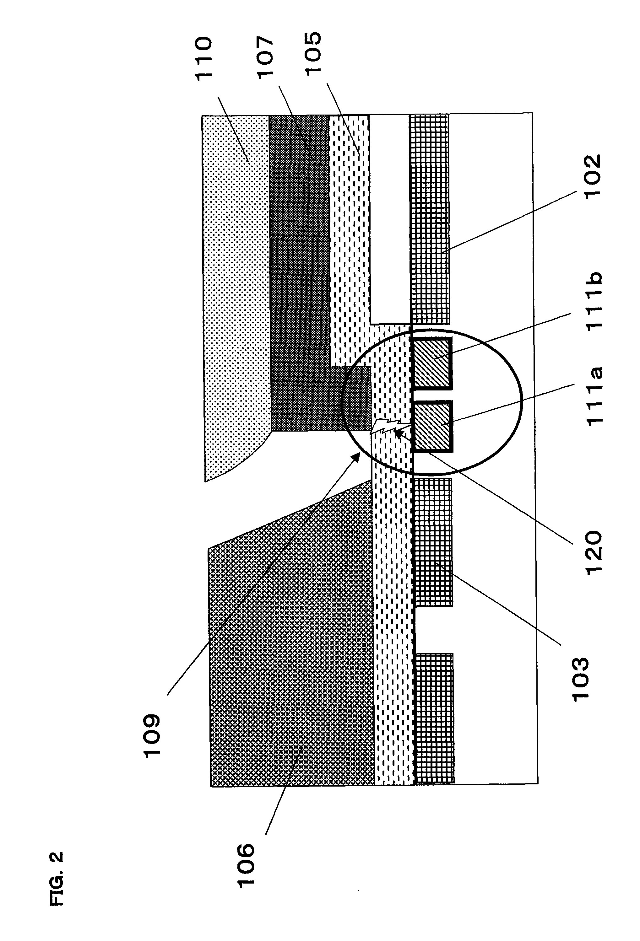
[0063]An electrode structure for a semiconductor chip according to a second embodiment of the present invention is the same as the electrode structure for the semiconductor chip according to the first embodiment described above except for a dummy pattern formed by the dummy metal. FIG. 5 is a diagram illustrating a bump electrode 500 of a semiconductor device according to the second embodiment of the present invention. In FIG. 5, the same components as shown in FIG. 1 are denoted by the same corresponding reference characters, and the description thereof is not given. In the bump electrode 500, a dummy metal 150 is provided in the uppermost layer portion of the silicon 101 between the pad-form wiring metal 102 and the wiring metal 103.

[0064]A dummy pattern of the electrode pad according to the second embodiment will be described below in detail. FIG. 6 is a diagram illustrating a dummy pattern of the electrode pad according to the second embodiment. In FIG. 6, the dummy metal 150 ha...

third embodiment

[0067]An electrode structure for a semiconductor chip according to a third embodiment of the present invention is the same as the electrode structure for the semiconductor chip according to the second embodiment described above except for a dummy pattern formed by the dummy metal. Hereinafter, a dummy pattern of an electrode pad according to the third embodiment will be described. FIG. 7 is a diagram illustrating a dummy pattern of an electrode pad according to the third embodiment. The dummy pattern according to the second embodiment as shown in FIG. 6 is formed such that the dummy metal 150 forms a continuous surface, whereas the dummy pattern shown in FIG. 7 is a honeycomb pattern in which a plurality of dummy metals 170 each having a regular hexagonal shape are continuously positioned.

[0068]As describe above, when the plurality of dummy metals 170 each having a regular hexagonal shape form a continuous surface, expansion of a crack generated due to bump stress concentrated on th...


PUM

PropertyMeasurementUnit
distanceaaaaaaaaaa
shapeaaaaaaaaaa
electric characteristicsaaaaaaaaaa

Abstract

The bump electrode 100 of the present invention has a structure in which dummy metals 111 are provided in the uppermost layer portion of a silicon 101 between a pad-form wiring metal 102 and a wiring metal 103 such that an edge of each dummy metal and an edge of the barrier metal 107 are not aligned in a line, and a lot of interfaces are formed between the dummy metals 111 and an interlayer film 140, and therefore expansion of a crack generated due to bump stress concentrated on the under-edge portion 109 below the barrier metal 107 between the pad-form wiring metal 102 and the wiring metal 103 is suppressed.

Description

BACKGROUND OF THE INVENTION[0001]1. Field of the Invention[0002]The present invention relates to an electrode structure for a semiconductor chip, and more particularly to an electrode structure for a semiconductor chip forming a flip-chip connection for suppressing expansion of a crack.[0003]2. Description of the Background Art[0004]A conventional structure of an electrode pad for a flip-chip connection in a semiconductor device will be described with reference to the drawings. FIG. 11A is a diagram illustrating a typical flip-chip connection structure. In FIG. 11A, a semiconductor chip 1101 and an interposer substrate 1102 are connected to each other through solder bumps. FIG. 11B is a cross-sectional view of the flip-chip connection structure shown in FIG. 11A along lines A-A′ of FIG. 11A. In FIG. 11B, the semiconductor chip 1101 and the interposer substrate 1102 are connected to each other through the solder bumps 1103, and an underfill resin 1104 covers a connecting portion of t...

Claims


Application Information

Patent Timeline
Patent Type & Authority Patents(United States)
IPC IPC(8): H01L23/485H01L29/40
CPCH01L24/11H01L2224/13099H01L2224/16H01L2924/01015H01L2924/01022H01L2924/01074H01L2924/01078H01L2924/01033H01L2924/014H01L2224/05022H01L2224/05001H01L2224/05572H01L2224/051H01L2224/05655H01L2224/05666H01L2224/05684H01L2224/05571H01L2224/13021H01L2224/02126H01L2224/05559H01L24/05H01L24/13H01L2224/06131H01L2224/06135H01L2924/00014
Inventor NAGAI, NORIYUKI
Owner PANASONIC SEMICON SOLUTIONS CO LTD
Why Eureka
Try Eureka