Phase change random access memory and layout method of the same

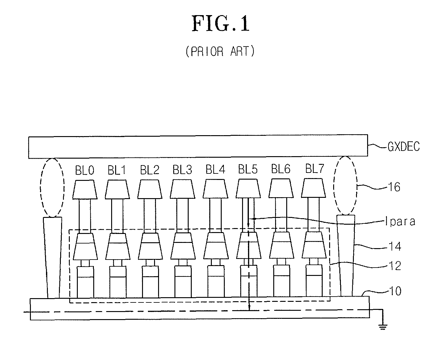
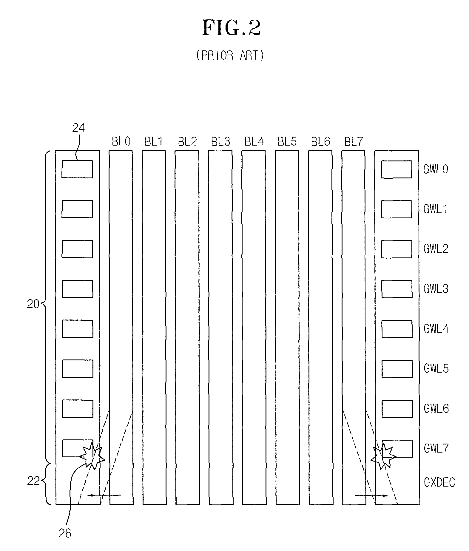
a random access memory and phase change technology, applied in the field of phase change random access memory (pram), can solve the problems of data access error, data access error, and difficulty in distinguishing between ‘1’ and ‘0’ in the data, so as to prevent data access error, prevent collapse of outermost bitlines, and remove parasitic current

Active Publication Date: 2011-02-08
SK HYNIX INC
View PDF13 Cites 4 Cited by
  • Summary
  • Abstract
  • Description
  • Claims
  • Application Information

AI Technical Summary

Benefits of technology

[0022]There is provided a PRAM capable of preventing data access error due to parasitic current generated in a dummy cell within a cell array.
[0023]Also, there is provided a PRAM capable of preventing electrical short between a bitline and a global wordline due to collapse of the bitline.
[0064]According to the present invention, since the dummy cells and the bitlines are electrically isolated from each other and thus the dummy cells are always maintained in a turn-off state, it is possible to remove parasitic current due to the dummy cells and thus prevent data access error.
[0065]According to the present invention, since regions of the outermost bitlines in the cell array, which correspond to the dummy cells, are extended to the outside, it is possible to prevent collapse of the outermost bitlines and thus prevent electrical short between the bitline and a global wordline.
[0066]According to the present invention, there is provided a PRAM that always maintains dummy cells in a turn-off state by supplying a voltage higher than the level of a bitline activation voltage to a dummy active region. Therefore, it is possible to prevent a data access error due to parasitic current generated in the dummy cells.

Problems solved by technology

However, since the dummy cell string 12 has, like other memory cells, a structure that is respectively electrically connected with the bitlines BL0˜BL7, there is a problem that when one bitline BL is selected, current Ipara may flow to the dummy active region 10 through a dummy cell electrically connected to the selected bitline BL.
Therefore, this is problematic in that a sense amplifier that senses and amplifies the data may malfunction, resulting in difficulty in distinguishment of ‘1’ and ‘0’ in the data.
However, in a dummy cell region 22, in which dummy cell strings (not shown) are disposed, the upper vias are not formed at the outside of the two outermost bitlines BL0, BL7 in order to electrically isolate the dummy cell string and a global row decoding line GXDEC, this results in problems in that the two bitlines BL0, BL7 may collapse in the direction shown in FIG. 2.
When the global wordline GWL7 and the bitline (for example, BL0) are electrically connected due to the collapse of the bitline BL0, there is a problem in that a data access error may occur because a direct current path is formed between the global wordline GWL7 and the bitline BL0.
Also, upon data access, for example, when the global wordline GWL7 is activated to a ground voltage VSS level and the bitline BL0 is activated to a boost voltage VPP level, there is a problem that consumption of the boost voltage VPP may be rapidly increased due to electrical short between the global wordline GWL7 and the bitline BL0.
Further, upon standby, for example, when the global wordline GWL7 is in an inactivated state at a boost voltage VPP level and the bitline BL0 is in an inactivated state at a ground voltage VSS level, there is a problem in that a leakage current may be rapidly increased due to electrical short between the global wordline GWL7 and the bitline BL0.
However, this proposed solution brings about additional problems, including an increase in the area of the cell array due to the addition of the dummy line.
However, extend the bitline sufficiently to prevent the pattern collapse is difficult because of the space between the bitline BL0, BL7 and the upper via 30, therefore there is a large possibility of electrical short between the bitline BL0, BL7 and the upper via 30 when the bitline BL0, BL7 is extended toward the upper via 30.

Method used


Image

  • Phase change random access memory and layout method of the same
  • Phase change random access memory and layout method of the same
  • Phase change random access memory and layout method of the same

Examples


Embodiment Construction

[0079]Hereinafter, preferred embodiments of the present invention will be described in detail with reference to the accompanying drawings.

[0080]In one embodiment of the present invention, a PRAM in which dummy cells and bitlines are electrically isolated from each other and regions of the bitlines disposed at the outermost in a cell array region, corresponding to the dummy cell, are extended to the outside and which is thus capable of removing parasitic current due to the dummy cells and preventing collapse of the outermost bitlines is disclosed.

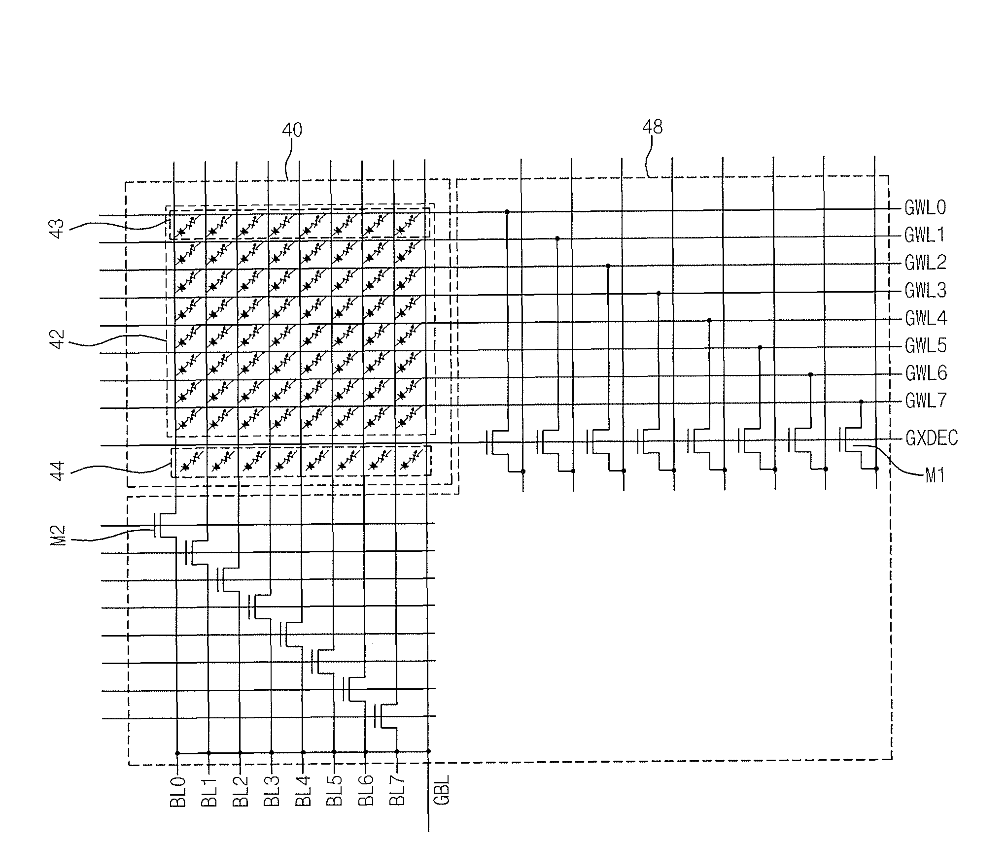
[0081]Specifically, according to the present embodiment, the PRAM includes a plurality of cell array units, each of which may include a cell array 40 and a cell array control unit 48 as shown in FIG. 4.

[0082]The cell array 40 includes a plurality of memory cell strings 42 and at least one dummy cell string 44.

[0083]Herein, each memory cell string 43 includes phase change memory cells. The phase change memory cells are arranged in the region ...


PUM


Abstract

A phase change random access memory (PRAM) includes a cell array divided into an active region and a dummy active region. A bitline is formed across the active region and the dummy active region and a global wordline is formed in the active region so as to intersect with the bitline. The cell array includes a phase change memory cell formed at an intersection point of the bitline and the global wordline that is electrically connected with the bitline and the global wordline. The cell array further includes a phase change dummy cell formed below the bitline in the dummy active region that is electrically isolated from the bitline. The dummy cell maintains a turn-off state as the dummy cell and the bitline are electrically isolated from each other.

Description

CROSS-REFERENCE TO RELATED APPLICATIONS[0001]The present application claims priority to Korean patent application numbers 10-2008-0023040 filed on Mar. 12, 2008 and 10-2008-0023042 filed on Mar. 12, 2008, both of which are incorporated herein by reference in their entirety.BACKGROUND OF THE INVENTION[0002]The present invention relates generally to a phase change random access memory (PRAM), and more particularly to a PRAM including dummy cells and a layout method of the same.[0003]In general, when forming memory cells of a PRAM, a cell array may be formed by repeated arrangement of memory cell strings including diodes formed by selective epitaxial growth.[0004]That is, in a single cell array, an 8-bit cell string may be arranged in a global wordline direction and a global row decoding line connected to a global row decoder (global X-decoder) together with the 8-bit cell strings may be arranged in a bitline direction.[0005]Herein, since the global row decoding line is used for the pu...

Claims


Application Information

Patent Timeline
Patent Type & Authority Patents(United States)
IPC IPC(8): G11C11/00
CPCG11C7/18G11C8/14G11C13/0004G11C13/0028H01L27/2409H01L27/2463H01L45/06H01L45/1233G11C2213/72H10B63/20H10B63/80H10N70/231H10N70/826
Inventor PARK, HAE CHAN
Owner SK HYNIX INC
Why Eureka
Try Eureka