Display device and display method

a display device and display method technology, applied in the field of display devices, can solve the problems of reducing power consumption, difficulty in setting a pause period, and reducing power consumption, so as to reduce the total amount of potential change, reduce the number of changes in potential for video signal lines, and reduce the power consumption for driving video signal lines

Inactive Publication Date: 2015-05-28
SHARP KK
View PDF4 Cites 19 Cited by
  • Summary
  • Abstract
  • Description
  • Claims
  • Application Information

AI Technical Summary

Benefits of technology

[0028]In the first aspect of the present invention, the order of selecting the scanning signal lines is determined such that at least two scanning signal lines being equal at each of the video signal lines in terms of a potential applied to the video signal line are selected at the same time, and therefore, the number of changes in potential for the video signal lines decreases compared to the case where the scanning signal lines are selected one by one in order of arrangement, resulting in a reduced total amount of change in potential. Thus, power consumption for driving the video signal lines can be reduced.
[0029]In the second aspect of the present invention, when the number of scanning signal lines being equal at each of the video signal lines in terms of the potential applied thereto exceeds a predetermined threshold, the order of selection is determined such that the same number of scanning signal lines as the threshold are selected at the same time, and therefore, the number of simultaneously selectable rows is limited. Thus, the drive capability of the video signal line drive circuit can be inhibited from being surpassed, thereby preventing display quality from being reduced.
[0030]In the third aspect of the present invention, the order of selection is determined such that at an immediately succeeding place within the order after the same number of scanning signal lines as the threshold have been selected at the same time, up to the same number of unselected remaining scanning signal lines as the threshold are selected at the same time, whereby the drive capability of the video signal line drive circuit can be inhibited from being surpassed, and further, the scanning signal lines selected at the immediately succeeding place within the order are equal at each of the video signal lines in terms of the potential applied to the video signal line, so that changes in potential for the video signal lines occur only to such a limited extent, resulting in reduced power consumption for driving the video signal lines.
[0031]In the fourth aspect of the present invention, a selection period for the scanning signal lines to be selected at the same time is set such that the selection period lasts longer as the number of scanning signal lines to be selected at the same time increases, and the selection period corresponding to the scanning signal lines to be selected at the same time is longer than a period in which one scanning signal line is selected, so that a sufficiently long charging time is ensured, whereby it is possible to inhibit the drive capability of the video signal line drive circuit from being surpassed, thereby preventing display quality from being reduced.
[0032]In the fifth aspect of the present invention, at least a part of the order is determined so as to minimize an integrated value obtained by adding up absolute values of respective amounts of change in potential for at least a part of the video signal lines due to switching among the scanning signal lines, resulting in reduced power consumption for driving the video signal lines.
[0033]In the sixth aspect of the present invention, the next scanning signal line to be selected is determined so as to minimize the integrated value obtained by adding up the absolute values of the amounts of change in potential, and a scanning signal line to be selected immediately thereafter is determined so as to minimize the integrated value obtained by adding up the absolute values of the amounts of change in potential, resulting in reduced power consumption for driving the video signal lines.

Problems solved by technology

In addition, each scanning signal line is selected for a shorter period of time, and therefore, there is difficulty in setting a pause period in which no scanning signal lines are selected during one frame period.
As a result, there is also difficulty in reducing power consumption by setting such a pause period.
In this configuration, no reset signal is provided to any pixel whose display state remains unchanged, resulting in reduced power consumption.

Method used


Image

  • Display device and display method
  • Display device and display method
  • Display device and display method

Examples


first embodiment

1. First Embodiment

[0065]

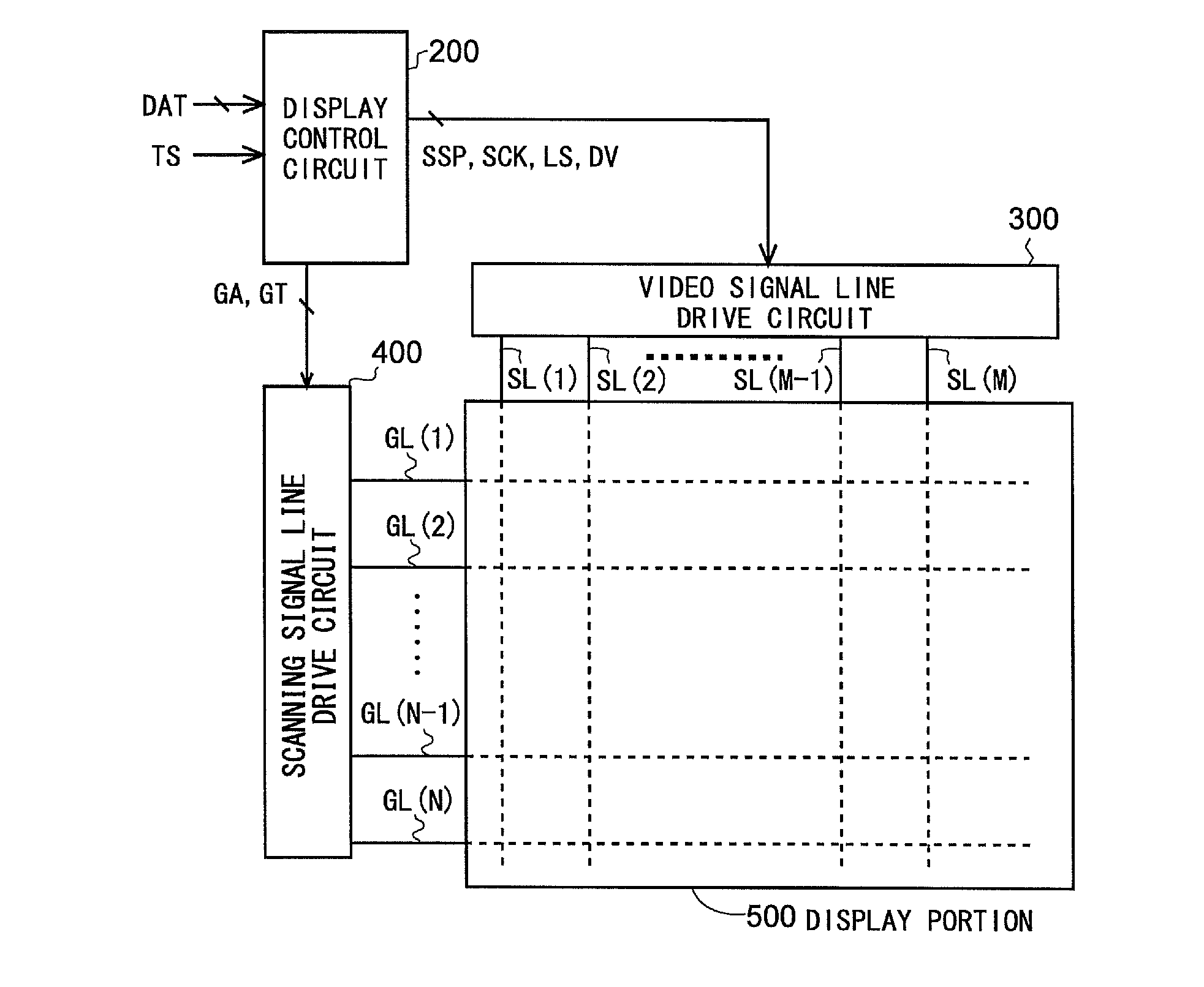
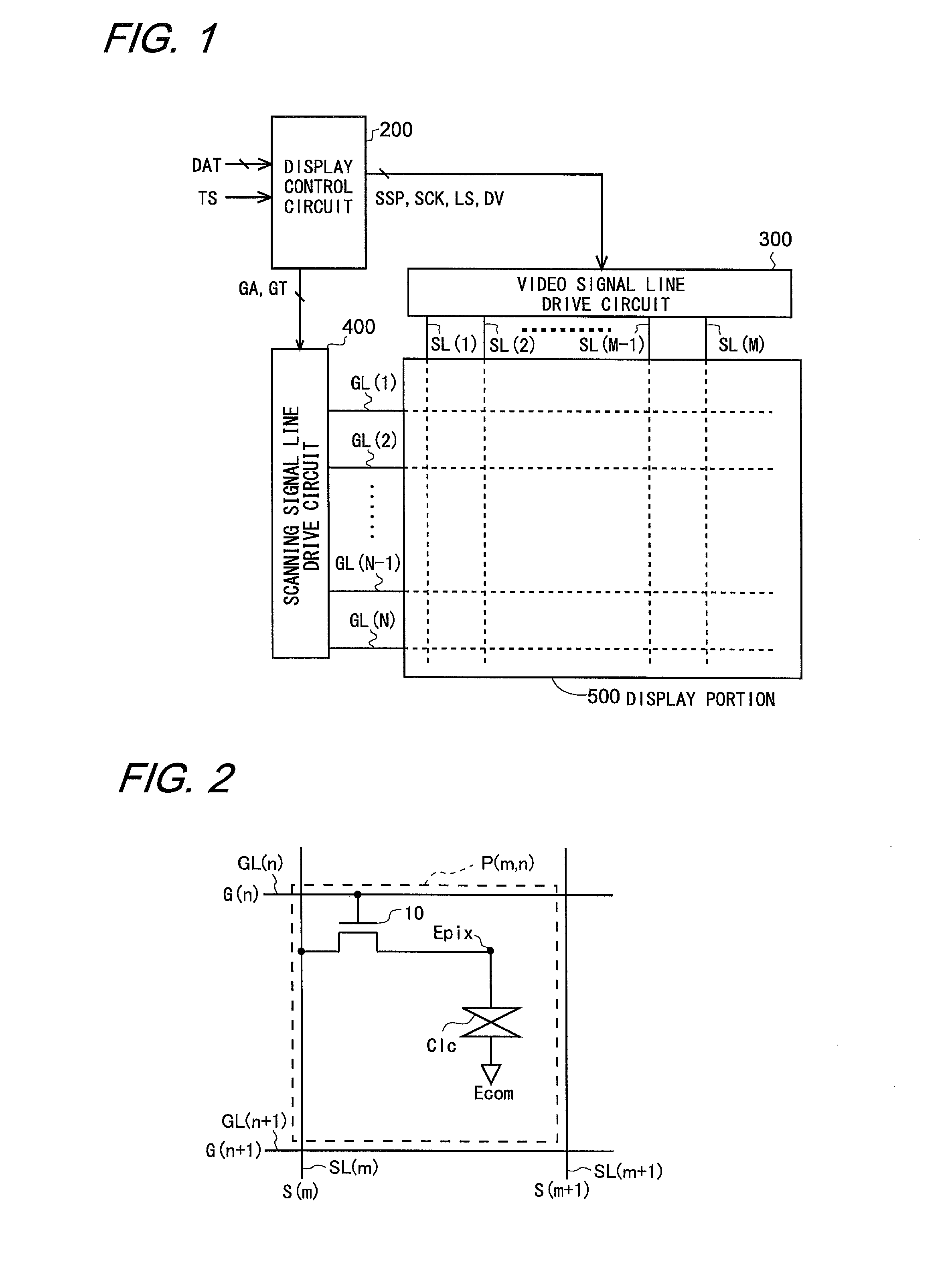
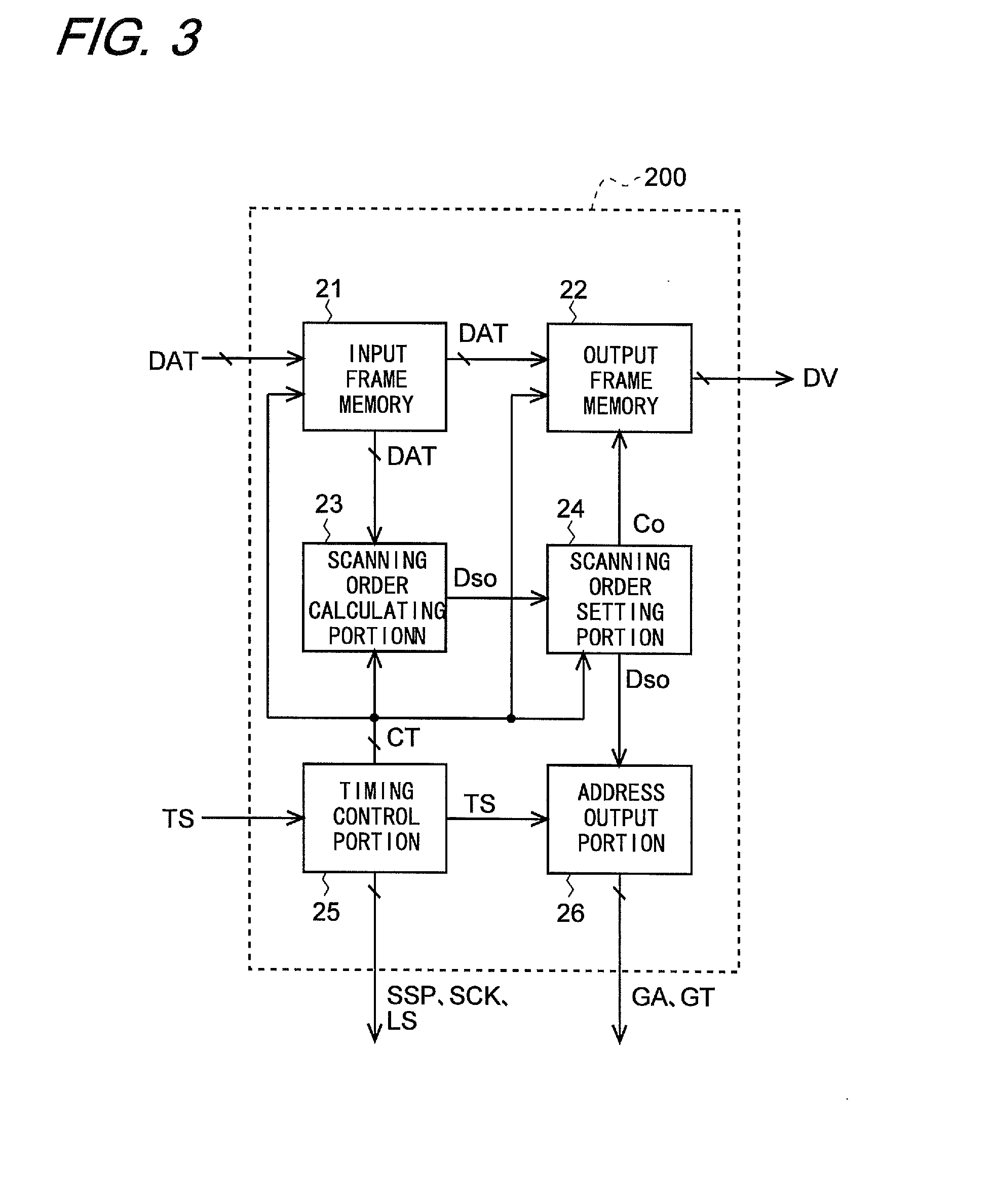
[0066]FIG. 1 is a block diagram illustrating the overall configuration of an active-matrix liquid crystal display device according to a first embodiment of the present invention. This liquid crystal display device includes a drive control portion consisting of a display control circuit 200, a video signal line drive circuit (source driver) 300, and a scanning signal line drive circuit (gate driver) 400, and also includes a display portion 500. The display portion 500 includes a plurality (M) of video signal lines SL(1) to SL(M), a plurality (N) of scanning signal lines GL(1) to GL(N), and a plurality (M×N) of pixel forming portions provided along the video signal lines SL(1) to SL(M) and the scanning signal lines GL(1) to GL(N). Note that in the following, a pixel forming portion provided near and in relation to the intersection of a scanning signal line GL(n) and a video signal line SL(m) (in the figure, near and to the lower right of the intersection) will...

second embodiment

2. Second Embodiment

[0140]

[0141]The configuration and operation of the display device in the present embodiment are approximately the same as those of the display device shown in FIGS. 1 and 2, the configuration and operation of the display control circuit in the present embodiment are approximately the same as those of the display control circuit 200 shown in FIG. 3, therefore, similar components are denoted by the same reference characters, and any descriptions about similar configurations and operations will be omitted.

[0142]The display control circuit 200 in the present embodiment outputs gate address signals GA after determining the order of selecting the scanning signal lines such that scanning signal lines corresponding to rows with the same display content are selected at the same time, and then determining addresses sequentially such that the scanning signal lines GL(1) to GL(N) are selected one by one or a plurality sets of rows with the same display content are selected s...

third embodiment

3. Third Embodiment

[0177]

[0178]An active-matrix liquid crystal display device according to the present embodiment operates in the same manner as the display device of the first embodiment shown in FIG. 1 and have the same configuration as the first or second embodiment except for some features of the display control circuit, therefore, the same components are denoted by the same characters, and any descriptions thereof will be omitted.

[0179]FIG. 20 is a block diagram illustrating the configuration of the display control circuit in the third embodiment of the present invention. As can be appreciated in comparison with the display control circuit 200 shown in FIG. 3, the display control circuit 250 shown in FIG. 20 operates in the same manner and has the same configuration except that a display transition detecting portion 28 is additionally provided, therefore, the same components are denoted by the same characters, any descriptions thereof will be omitted, and only the operation of ...


PUM


Abstract

When there are a plurality of rows with the same display content, a scanning order calculating portion (23) provided in a display control circuit (200) determines addresses sequentially such that scanning signal lines corresponding to the rows are selected at the same time. A scanning order setting portion (24) controls an address output portion (26) such that the scanning signal lines are selected in such an order, and also controls digital image signals DV outputted by output frame memory (22). In this case, the number of changes in potential for video signal lines can be reduced by the number of rows selected at the same time, resulting in reduced power consumption for driving the video signal lines.

Description

TECHNICAL FIELD[0001]The present invention relates to display devices, more specifically to an active-matrix display device and a display method in which scanning is performed in a different manner from sequential scanning.BACKGROUND ART[0002]Recent liquid crystal display devices have higher definition screens and therefore have increased numbers of video signal lines and scanning signal lines. Accordingly, more power is required for driving these signal lines. In addition, each scanning signal line is selected for a shorter period of time, and therefore, there is difficulty in setting a pause period in which no scanning signal lines are selected during one frame period. As a result, there is also difficulty in reducing power consumption by setting such a pause period.[0003]Therefore, Japanese Laid-Open Patent Publication No. 2005-265869 discloses the configuration of a liquid crystal display device in which reset signals are provided only to scanning signal lines through which pixe...

Claims


Application Information

Patent Timeline
Patent Type & Authority Applications(United States)
IPC IPC(8): G09G3/36
CPCG09G3/3659G09G3/3688G09G2310/027G09G2310/06G09G2330/023G09G2310/0213G09G3/2092G09G3/2096G09G3/3233G09G3/3291G09G2310/0205G09G2310/0227G09G2310/04G09G2370/08
Inventor MAEDA, KAZUHIRONAKAGAWA, YOUSUKE
Owner SHARP KK
Why Eureka
Try Eureka