

Light-emitting device, wavelength conversion member, phosphor composition and phosphor mixture
a technology of light-emitting devices and wavelength conversion members, applied in the direction of semiconductor devices, luminescent compositions, chemistry apparatuses and processes, etc., to achieve the effects of high total luminous flux, high emission efficiency and color rendering properties, and excellent binning characteristics
- Summary
- Abstract
- Description
- Claims
- Application Information
AI Technical Summary
Benefits of technology
Problems solved by technology
Method used
Image

Examples
examples
[0610]The present invention will be explained next in further detail on the basis of Examples and simulations, but the present invention is not limited to the embodiments below alone.
first embodiment
1. First Embodiment
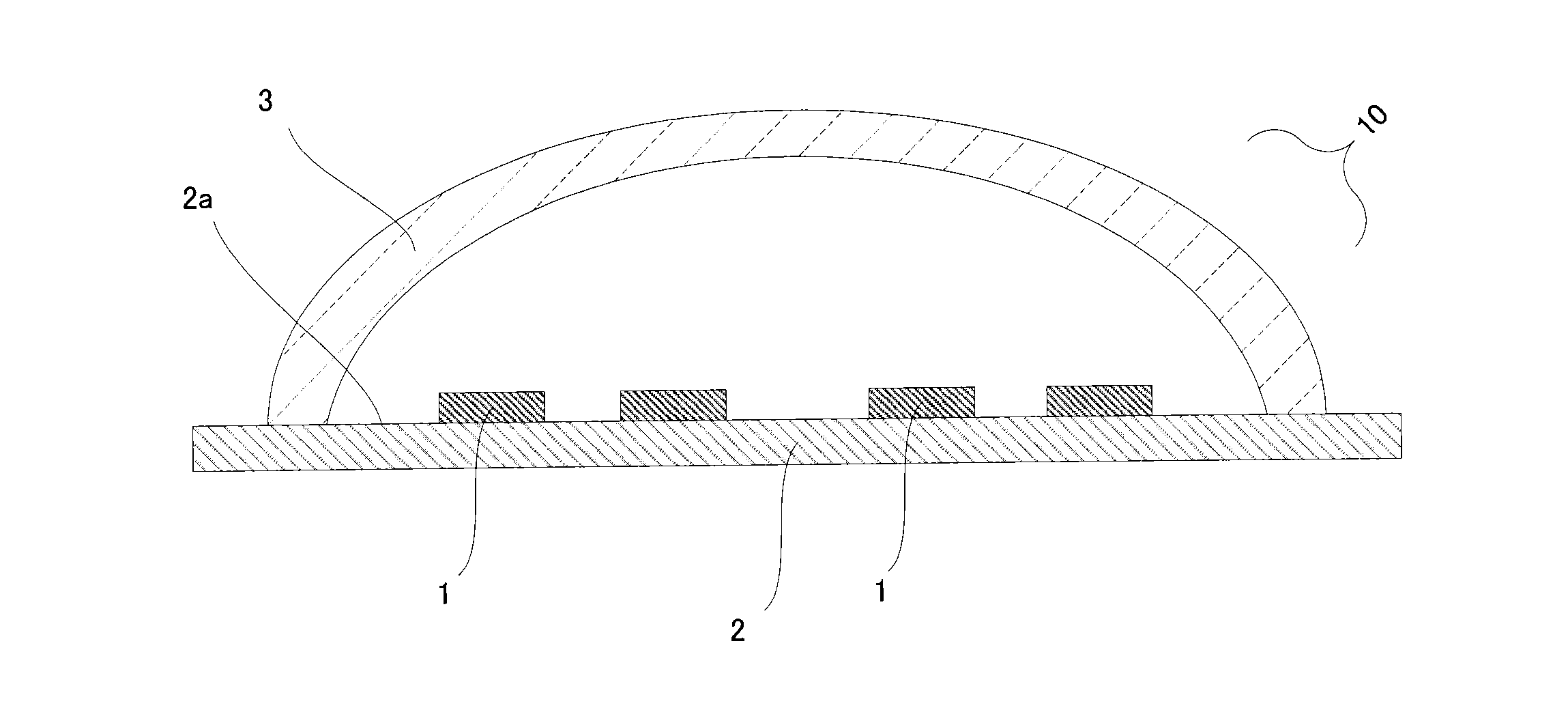
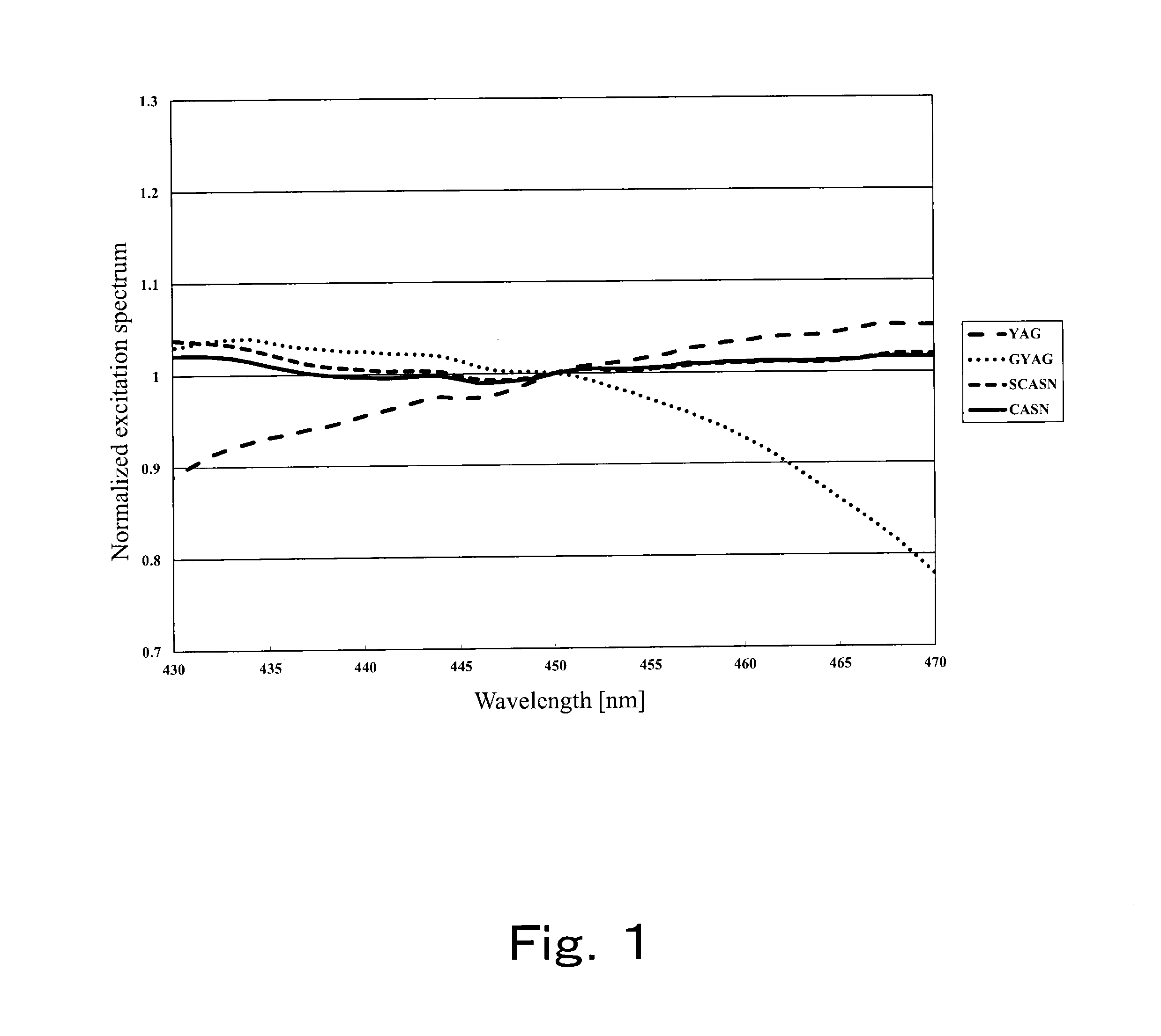
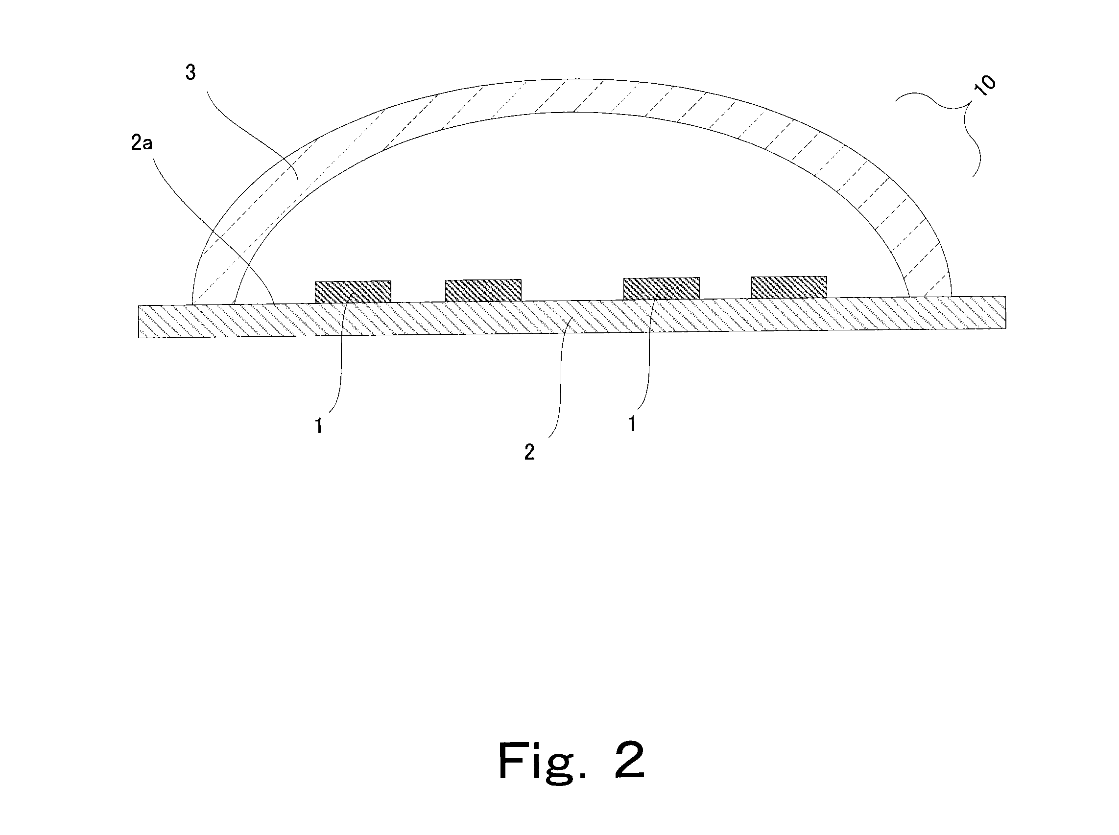
[0611]
[0612]FIG. 4 and Table 3 are results of simulations, by the inventors, of instances where phosphors represented by formula (m1) are used. The figure and the table illustrate the way in which color rendering properties and emission efficiency of light emitted by the light-emitting device vary depending on the type of phosphor.
[0613]For the simulations, respective wavelength conversion members were configured using a chip having a peak wavelength of 453 nm as an excitation source, and using three types of phosphor from among four types of phosphor, namely YAG, GYAG, SCASN and CASN (relying on the actually measured data of, for instance, emission spectra of phosphors used in the Experimental Examples described below). The way in which the relationship between color rendering properties and emission efficiency varies was simulated through adjustment of the content of the phosphors, in such a manner that the emission color of the respective wavelength conversion ...
second embodiment
2. Second Embodiment
[0677]The explanation on the Examples of the first embodiment described above applies to the Examples of the present embodiment.
PUM
| Property | Measurement | Unit |
|---|---|---|
| emission wavelength | aaaaa | aaaaa |
| emission wavelength | aaaaa | aaaaa |
| peak wavelength | aaaaa | aaaaa |
Abstract
Description
Claims
Application Information