Air gap structure integration using a processing system

Active Publication Date: 2015-06-18
APPLIED MATERIALS INC
View PDF3 Cites 64 Cited by
  • Summary
  • Abstract
  • Description
  • Claims
  • Application Information

AI Technical Summary

Benefits of technology

[0010]In one embodiment, a method for forming an air gap structure in a integrated layer stack includes dry etching a mold layer disposed on the integrated layer stack in a processing system under vacuum. The mold layer is disposed between one or more interconnects, and the process of dry etching of the mold layer exposes at least a portion of the one or more of the interconnects. The method also includes depositing a liner layer over the exposed portion of the one or more interconnects. The method disclosed herein is generally performed in the processing system without breaking vacuum.
[0011]In another embodiment, a method for forming an air gap structure in a integrated layer stack includes dry etching an mold layer disposed on the integrated layer stack in a first processing chamber in a processing system under vacuum. The mold layer is disposed between one or more copper interconnects, and the process of dry etching of the mold layer exposes at least a portion of the one or more of the interconnects. The method also includes depositing a low-k material liner layer having a thickness of le

Problems solved by technology

Integrated circuits have evolved into complex devices that can include millions of components (e.g., transistors, capacitors and resistors) on a single chip.
At sub-micron dimensions, capacitive coupling potentially occurs between adjacent metal interconnects, which may cause cross talk and/or resistance-ca

Method used


Image

  • Air gap structure integration using a processing system
  • Air gap structure integration using a processing system
  • Air gap structure integration using a processing system

Examples


Embodiment Construction

[0021]In the following description, for purposes of explanation, numerous specific details are set forth in order to provide a thorough understanding of embodiments of the present disclosure. In some instances, well-known structures and devices are shown in block diagram form, rather than in detail, in order to avoid obscuring embodiments of the present disclosure. These embodiments are described in sufficient detail to enable those skilled in the art to practice embodiments of the present disclosure, and it is to be understood that other embodiments may be utilized and that logical, mechanical, electrical, and other changes may be made without departing from the scope of the present disclosure.

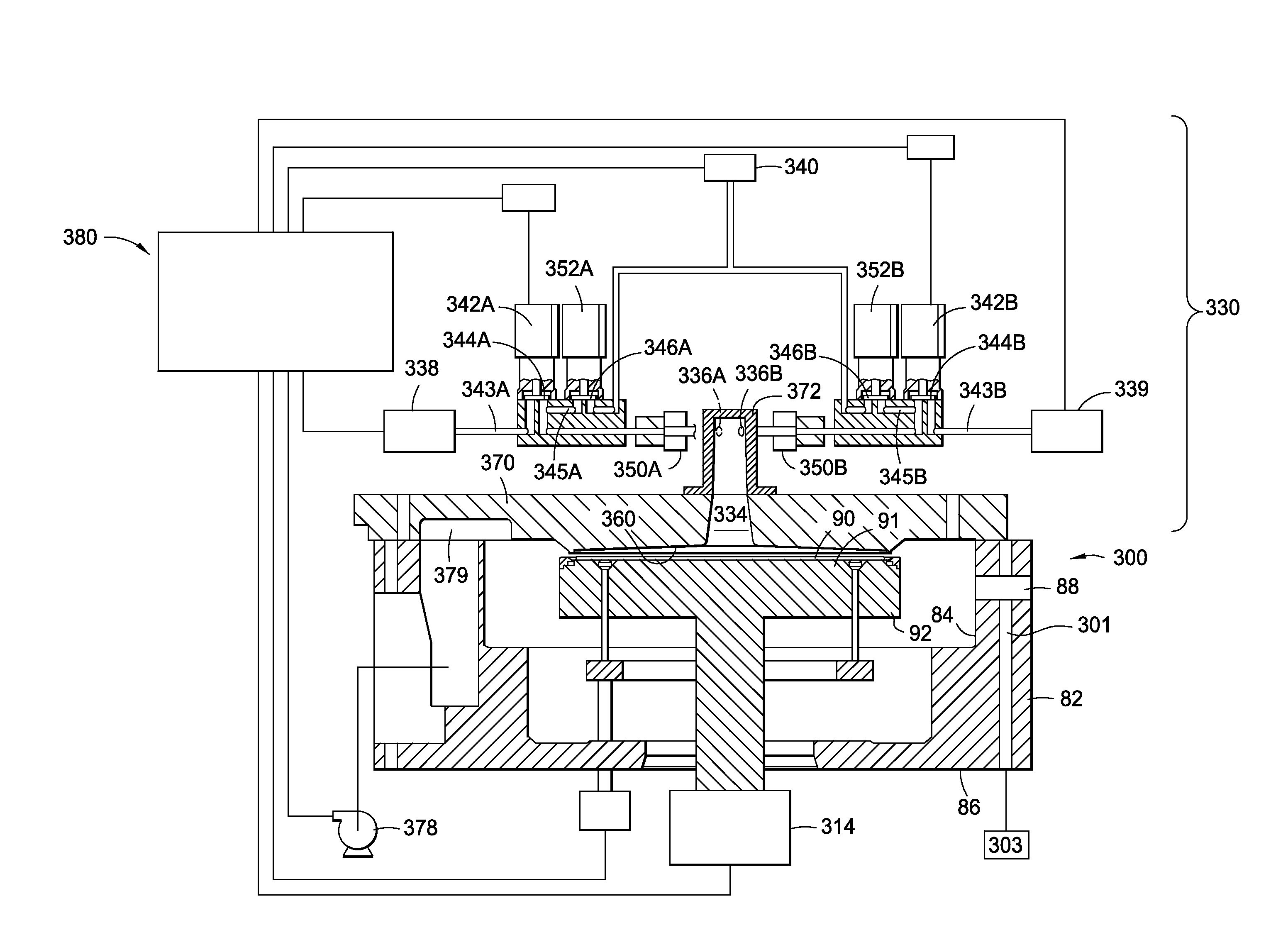
[0022]Embodiments described herein generally relate to air gap structure integration methods using a process system. More specifically, embodiments of the present disclosure relate to mold layer etching processes and liner deposition processes that are integrated within a processing system fo...


PUM

PropertyMeasurementUnit
Thicknessaaaaaaaaaa
Pressureaaaaaaaaaa
Dielectric polarization enthalpyaaaaaaaaaa

Abstract

A method for forming an air gap structure in an integrated layer stack includes dry etching a mold layer disposed on the stack in a processing system under vacuum. The mold layer is disposed between one or more interconnects, and the process of dry etching of the mold layer exposes at least a portion of the interconnects. The method also includes depositing a liner layer over the exposed portion of the interconnects. In another embodiment, a method for forming an air gap structure in an integrated layer stack includes dry etching an oxide mold layer disposed on the stack in an a first processing chamber in a processing system under vacuum. The method also includes depositing a low-k material liner layer over the interconnects, wherein the liner has a thickness of less than about 2 nanometers. The methods disclosed herein are performed in a processing system without breaking vacuum.

Description

CROSS-REFERENCE TO RELATED APPLICATIONS[0001]This application claims benefit from U.S. Provisional Patent Application No. 61 / 916,726, filed Dec. 16, 2013, which is incorporated by reference in its entirety.BACKGROUND[0002]1. Field[0003]Embodiments of the present disclosure generally relate to the formation of a dielectric layer structure that includes an air gap structure using an integrated processing system.[0004]2. Description of the Related Art[0005]Integrated circuits have evolved into complex devices that can include millions of components (e.g., transistors, capacitors and resistors) on a single chip. The demand for greater circuit density necessitates a reduction in the dimensions of the integrated circuit components, e.g., sub-micron dimensions and the use of various materials to fabricate devices in order to achieve much faster and better electrical performance, such as materials with higher conductivity used to form metal lines, materials with lower permittivity (low-k) d...

Claims


Application Information

Patent Timeline
IPC IPC(8): H01L21/768H01L21/311H01L21/02
CPCH01L21/31116H01L21/0217H01L21/76819H01L21/02167H01L21/76832H01L21/7682C23C16/303C23C16/36H01J37/32082H01L21/31138H01L21/76834
Inventor NAIK, MEHUL B.REN, HECUI, ZHENJIANG
Owner APPLIED MATERIALS INC
Why Eureka
Try Eureka