
Transparent electronic display board and method for manufacturing same

a technology of electronic display board and transparent material, which is applied in the direction of identification means, instruments, lighting and heating apparatus, etc., can solve the problems of short lifetime, low intensity of illumination, and high power consumption of electronic display board, so as to improve the image quality of video, reduce the distance between the light-emitting elements, and improve the effect of light density

Active Publication Date: 2015-06-25
G SMATT
View PDF5 Cites 3 Cited by
  • Summary
  • Abstract
  • Description
  • Claims
  • Application Information

AI Technical Summary

Benefits of technology

The present invention mounts light-emitting elements on two transparent plates that face each other, allowing for increased density of light and reduced distance between the elements. This results in improved image quality for videos.

Problems solved by technology

Neon lamps or CCLs use high voltage power and thus have disadvantages of high power consumption, risks of electric shock or fire, and a short lifetime.
On the other hand, EEFLs or CCFLs have problems in being used outdoor because they use high frequency.
Furthermore, EEFLs or CCFLs have disadvantages of low intensity of illumination and a short lifetime.
However, the above-mentioned light emitting devices are limited in enhancing aesthetic effects because of the size of a lamp or the size of a stand for supporting a light emitting device.
Thus, the number of light-emitting elements is limited.
As such, the conventional transparent electronic display board is problematic in that there is a limit in reducing the distance between the light-emitting elements because the arrangement of the transparent electrodes and the areas for installation of the light-emitting elements are taken into account.

Method used


Image

  • Transparent electronic display board and method for manufacturing same
  • Transparent electronic display board and method for manufacturing same
  • Transparent electronic display board and method for manufacturing same

Examples


Embodiment Construction

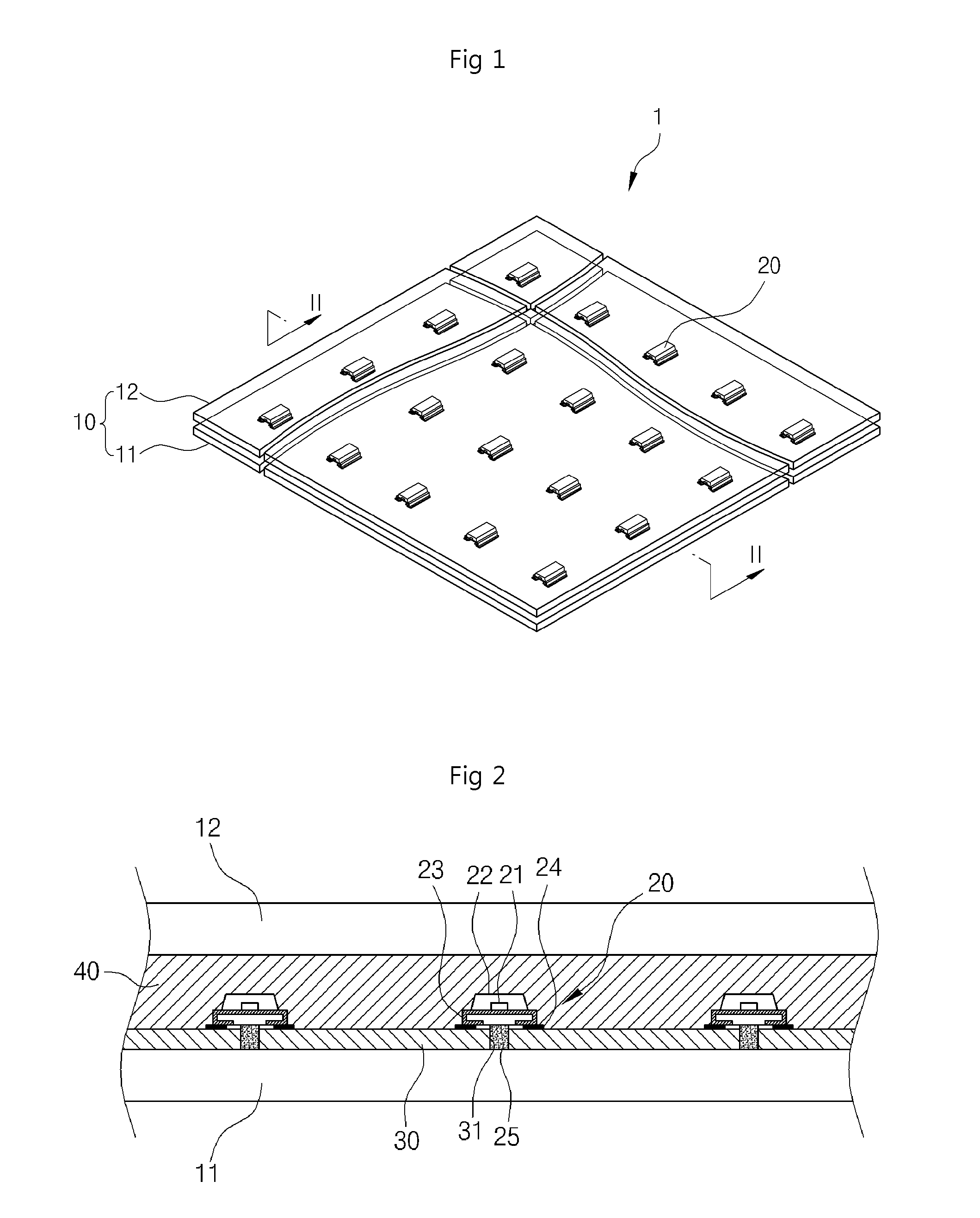
[0037]Hereinafter, a transparent electronic display board and a method of manufacturing the same according to the present invention will be described in detail with reference to the attached drawings.

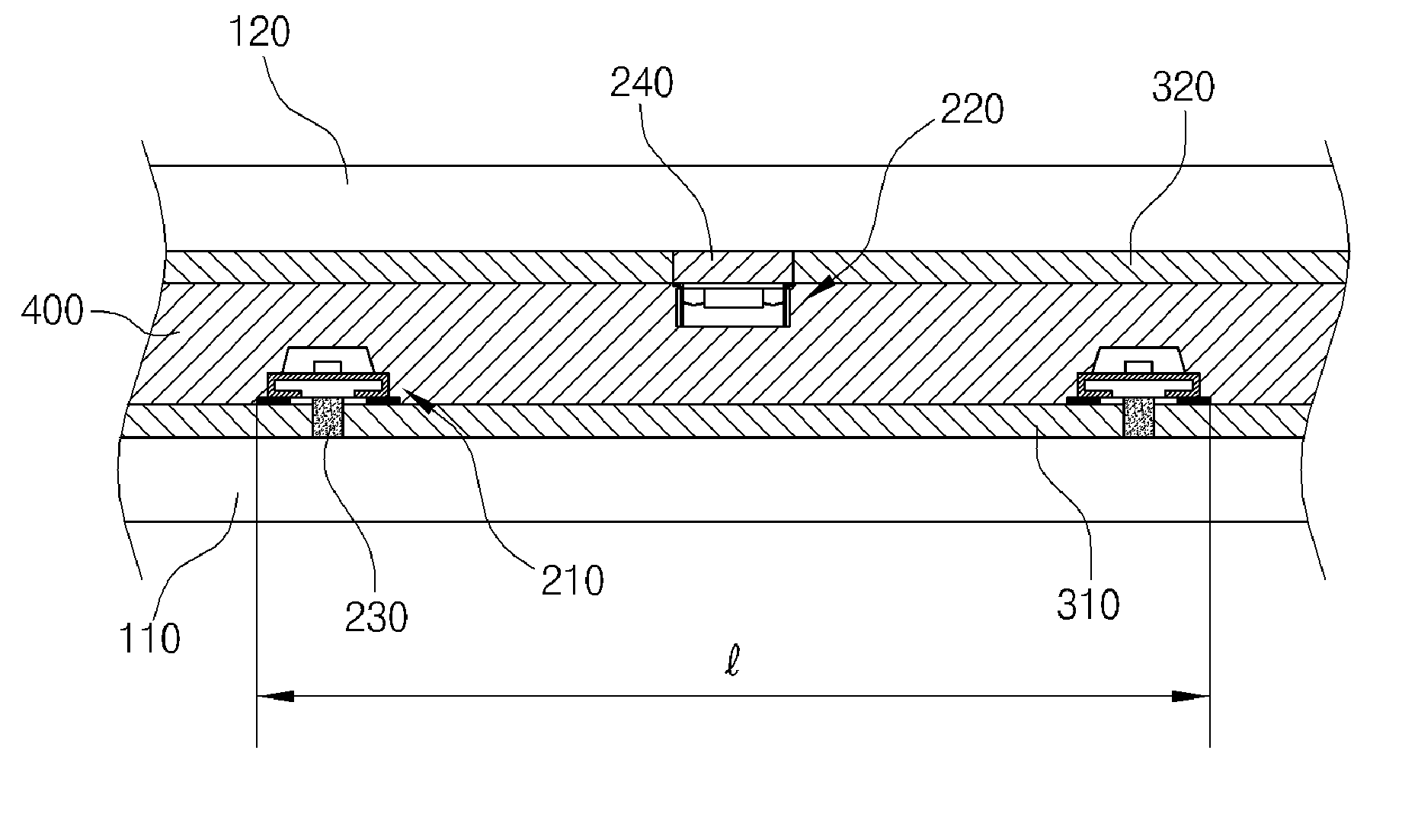
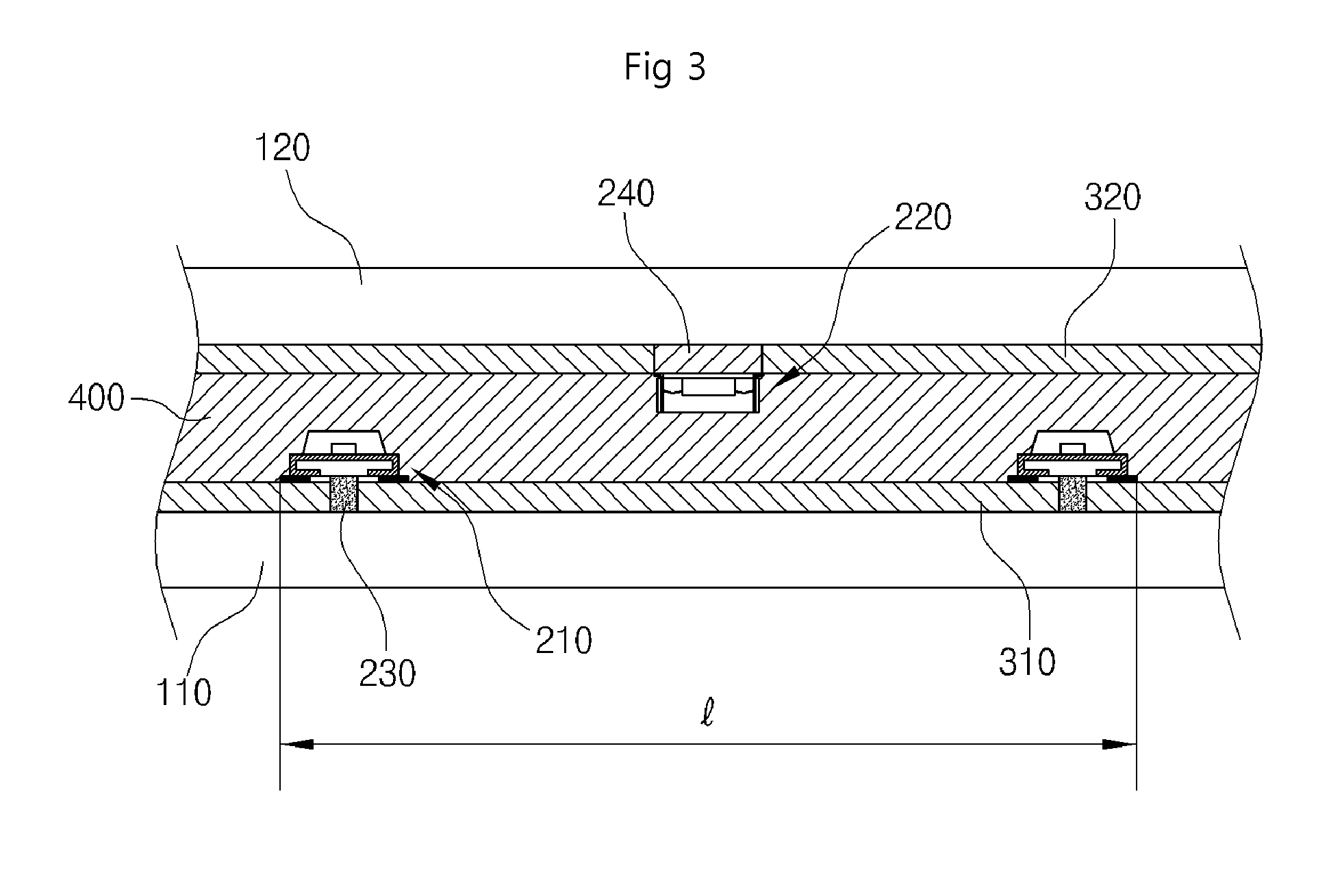
[0038]FIG. 3 is a sectional view illustrating a transparent electronic display board according to the present invention.

[0039]Referring to FIG. 3, the transparent electronic display board according to the present invention includes: a pair of transparent plates 110 and 120 including a first transparent plate 110 and a second transparent plate 120 that are spaced apart from each other by a predetermined distance; a first transparent electrode 310 fastened to an upper surface of the first transparent plate 110 of the transparent plates 110 and 120; a second transparent electrode 320 fastened to a surface of the second transparent plate 120; a first light-emitting element 210 connected to the first transparent electrode 310; a second light-emitting element 220 connected to the second trans...


PUM

PropertyMeasurementUnit
transparentaaaaaaaaaa
voltageaaaaaaaaaa
frequencyaaaaaaaaaa

Abstract

The present invention relates to a transparent electronic display board and a method of manufacturing the same. More particularly, the transparent electronic display board uses front light-emitting elements and rear light-emitting elements and / or both-sided light-emitting elements, whereby the number of light-emitting elements that can be installed in the transparent electronic display board can be increased. Thereby, the quality of an image displayed on the transparent electronic display board can be markedly improved.

Description

TECHNICAL FIELD[0001]The present invention generally relates to transparent electronic display boards and methods of manufacturing the same. More particularly, the present invention relates to a transparent electronic display board that uses front light-emitting elements and rear light-emitting elements and / or both light-emitting elements so that the number of light-emitting elements that can be installed in the electronic display board can be increased, whereby the quality of an image displayed on the electronic display board can be improved, and to a method of manufacturing the transparent electronic display board.BACKGROUND ART[0002]Generally, light emitting devices such as neon lamps, CCLs (cold cathode lamps), LEDs (light emitting diodes), etc. are widely used in outdoor electronic display boards. EEFLs (external electrode fluorescent lamps), CCFLs (cold cathode fluorescent lamps), LED electronic displays, etc. are used as indoor light emitting devices.[0003]Neon lamps or CCLs ...

Claims


Application Information

Patent Timeline
Patent Type & Authority Applications(United States)
IPC IPC(8): F21K99/00B32B37/02B32B37/16H01L33/42
CPCF21K9/10H01L33/42B32B37/02B32B2457/20F21K9/90B32B2307/412B32B2307/202B32B37/16G09F9/33F21K9/20G02F1/133603
Inventor LEE, HO JUN
Owner G SMATT
Learn More