Conductive film, display device and touch panel comprising same, and conductive film pattern determination method

a display device and touch panel technology, applied in the direction of instruments, computing, electric digital data processing, etc., can solve the problems of inability to take into account, limitation in inhibiting moire, and improvement of appearance of moire, so as to prevent impairment of image quality, improve appearance of moire, and improve visibility.

Active Publication Date: 2015-07-02
FUJIFILM CORP
View PDF2 Cites 10 Cited by
  • Summary
  • Abstract
  • Description
  • Claims
  • Application Information

AI Technical Summary

Benefits of technology

[0073]As described above, according to the present invention, even when a conductive film is installed and used on a display unit of a display device having a backlight unit that uses a prism sheet, the occurrence of moire can be suppressed, and visibility can be greatly improved.
[0074]That is, in the present invention, a difference of the peak spatial frequencies of spectrum peaks up to the second-order term of two-dimensional Fourier spectra of the microprism array pattern of the prism sheet and the wiring pattern of the conductive film, which is obtained by frequency analysis, is limited to a numerical value greater than a predetermined value such that the appearance of moire becomes excellent. Consequentially, it is possible to prevent impairment of image quality caused by the occurrence of moire, and to obtain excellent visibility. Furthermore, in the present invention, the lowest frequency of second moires, which are visually recognized due to the interference between two frequency peaks of moires occurring due to the interference among the microprism array pattern of the prism sheet, the wiring pattern of the conductive film, and the pixel array pattern of the display device, is limited such that it becomes higher than the lowest frequency of third moires occurring due to the interference between the wiring pattern and the pixel array pattern. Therefore, it is possible to prevent impairment of image quality caused by the occurrence of moire, and to obtain excellent visibility.
[0075]Particularly, in a case in which a conductive film is used as an electrode for a touch panel, according to the present invention, it is possible to suppress moire, which greatly impairs image quality when the conductive film is superimposed on a black matrix of a display unit of a display device including a backlight unit using a prism sheet and visually recognized, and to greatly improve visibility of display on the touch panel.

Problems solved by technology

Incidentally, for example, the out-cell mode, in which a touch sensor (touch panel) is mounted on pixel arrays of a display unit including a backlight using a prism sheet, has a problem in that moire occurring due to interference among the pixel arrays, the prism sheet, and the touch sensor should be taken into consideration.
However, because the technique is merely focused on moire occurring due to the interference between BM of the display and the wiring pattern of the conductive film, moire occurring by interference between a prism pattern of a prism sheet or the like, which is used in a lighting device such as a back light of a display, and BM or a wiring pattern is not taken into consideration at all.
Therefore, the technique has problems in that the occurrence of moire caused by interference with a prism pattern cannot be inhibited, moire is visually recognized, and improvement of appearance of moire is unsatisfactory.
Accordingly, the technique has a problem in that it has a limitation in inhibiting the moire occurring due to interference of a mesh-like pattern such as a wiring pattern.
As a result, the document has a problem in that it has nothing to do with inhibiting moire occurring by interference between an opaque wiring pattern and a prism pattern and interference among three patterns including an opaque wiring pattern, a pixel array pattern, and a prism pattern, and improving appearance of moire.

Method used


Image

  • Conductive film, display device and touch panel comprising same, and conductive film pattern determination method
  • Conductive film, display device and touch panel comprising same, and conductive film pattern determination method
  • Conductive film, display device and touch panel comprising same, and conductive film pattern determination method

Examples


first embodiment

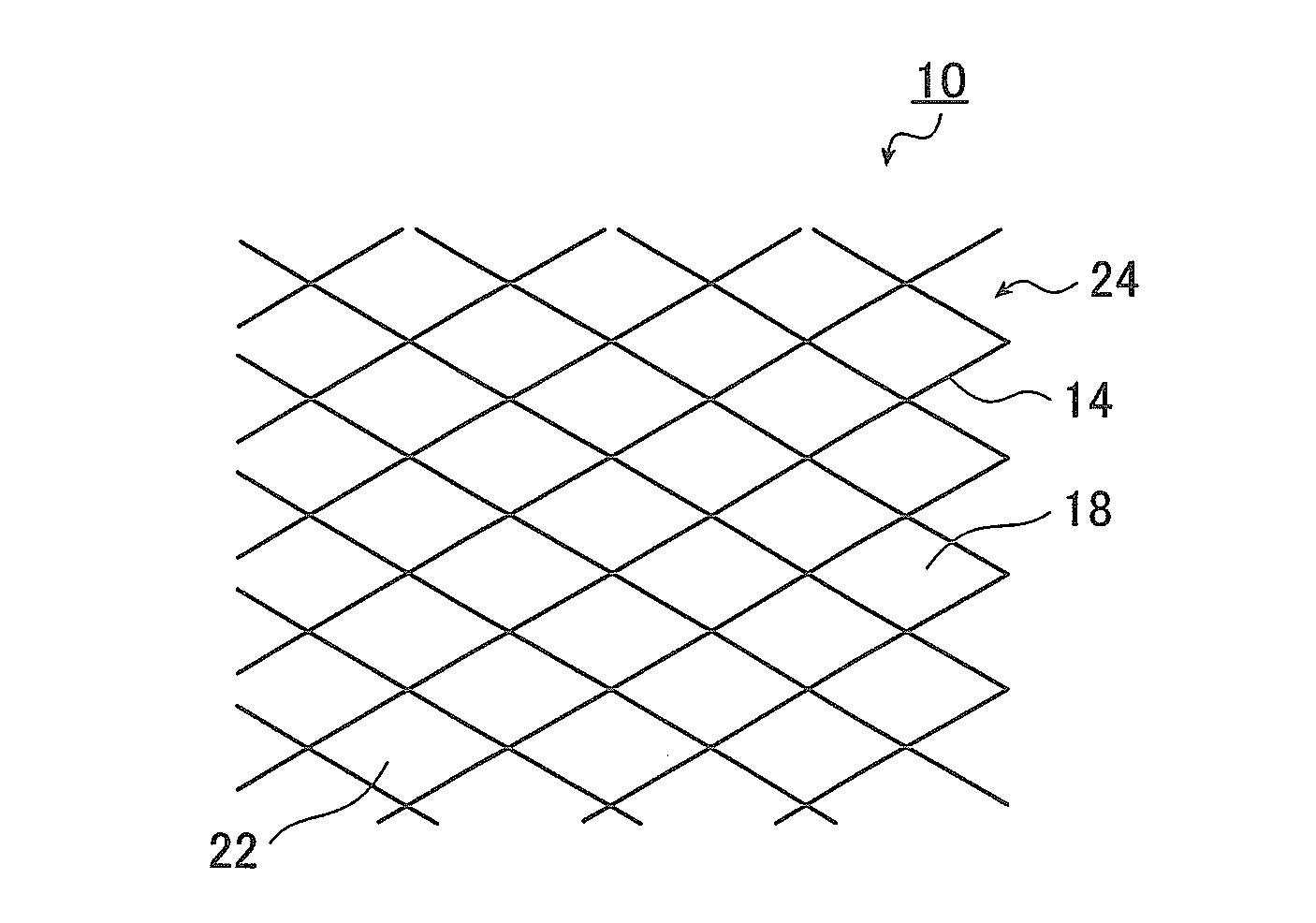
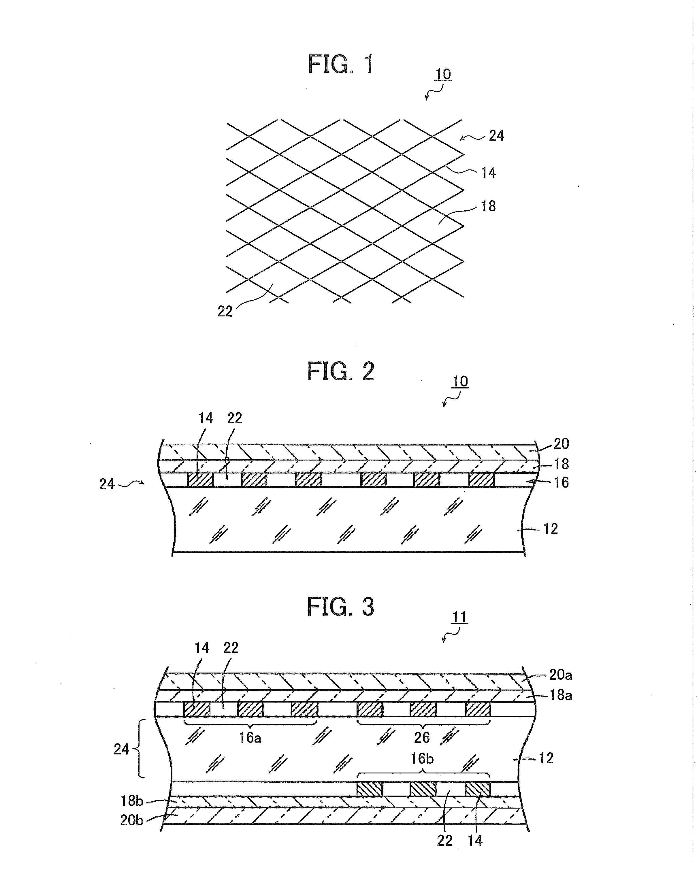
[0099]FIG. 1 is a partial enlarged plan view schematically showing an example of a conductive film according to the present invention, and FIG. 2 is a schematic partial cross-sectional view of the conductive film. Herein, FIG. 1 is an enlarged view showing a part of a wiring pattern of a mesh shape of the conductive film of the present embodiment.

[0100]As shown in these views, a conductive film 10 of the present embodiment is to be installed on a display unit of a display device including a backlight using a prism sheet. It is a conductive film having a wiring pattern excellent in suppressing the occurrence of moire with respect to a microprism array pattern (hereinafter, referred to as a “prism pattern”) of a prism sheet and a black matrix (BM) of a display unit. Particularly, it is a conductive film having a wiring pattern optimized in terms of moire appearance with respect to the prism pattern and a black matrix pattern (hereinafter, referred to as a “BM pattern”) when being supe...

second embodiment

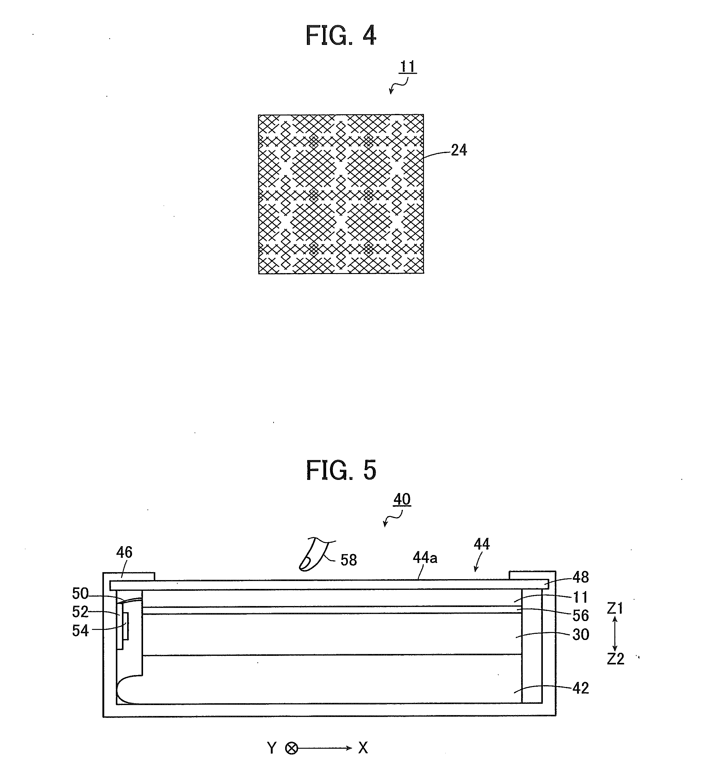
[0110]As shown in FIG. 3 and FIG. 4, the conductive film 11 includes a first conductive portion 16a and a dummy electrode portion 26 formed on one surface (on the upper side of FIG. 3) of the transparent substrate 12, a second conductive portion 16b formed on the other surface (on the lower side of FIG. 3) of the transparent substrate 12, a first protective layer 20a bonded to the substantially entire surface of the first conductive portion 16a and the first dummy electrode portion 26 through a first adhesive layer 18a, and a second protective layer 20b boned to the substantially entire surface of the second conductive portion 16b through a second adhesive layer 18b.

[0111]In the conductive film 11, the first conductive portion 16a and the dummy electrode portion 26 each include plural thin metal wires 14 and are formed on one surface (on the upper side of FIG. 3) of the transparent substrate 12, and the second conductive portion 16b includes plural thin metal wires 14 and is forme...


PUM


Abstract

This conductive film has a difference of over 3 cycles/mm between a peak spatial frequency for a plurality of spectral peaks in a two dimensional Fourier spectrum for transmittance image data for a wiring pattern and a peak spatial frequency for spectral peaks up to the second term in a two dimensional Fourier spectrum for transmittance image data for a microprism array pattern for a prism sheet on the display unit side of a backlight unit, for a first moire obtained by interference between a wiring pattern for a conductive section and the microprism array pattern. As a result, this conductive film is capable of suppressing the occurrence of moire and can greatly improve visibility, even when arranged upon a display unit having a backlight unit using a prism sheet.

Description

CROSS-REFERENCE TO RELATED APPLICATIONS[0001]This application is a Continuation of PCT International Application No. PCT / JP2013 / 073130 filed on Aug. 29, 2013, which claims priority under 35 U.S.C. §119(a) to Japanese Application No. 2012-197815 filed on Sep. 7, 2012. The above application is hereby expressly incorporated by reference, in its entirety, into the present application.BACKGROUND OF THE INVENTION[0002]The present invention relates to a conductive film, a display device and a touch panel each comprising the conductive film, and a conductive film pattern determination method.[0003]Examples of a conductive film installed on a display unit of a display device (hereinafter, also referred to as a display) include a conductive film for electromagnetic wave-shielding and a conductive film for a touch panel (for example, see JP 2009-117683 A, JP 2002-351341 A and JP 2000-206529 A).[0004]JP 2009-117683 A filed by the applicant of the present application discloses that a second patt...

Claims


Application Information

Patent Timeline
Patent Type & Authority Applications(United States)
IPC IPC(8): G06F3/044
CPCG06F3/044G06F3/0412G06F2203/04112G06F3/0443G06F3/0445G06F3/0446G02F1/1335G02F1/1343
Inventor IWAMI, KAZUCHIKA
Owner FUJIFILM CORP
Why Eureka
Try Eureka