Imaging device and imaging system

a technology of imaging system and imaging device, which is applied in the direction of television system, radioation control device, television system scanning details, etc., can solve the problem of difficult to obtain accurate image signals, and achieve the effect of reducing the optical path differen

Active Publication Date: 2015-07-23
CANON KK
View PDF3 Cites 2 Cited by
  • Summary
  • Abstract
  • Description
  • Claims
  • Application Information

AI Technical Summary

Benefits of technology

[0006]It has been found desirable to suppress incident light into a light-shielded pixel region that has been shielded, from the side of a light-sensing pixel region, and also reduce the optical path difference regarding incident light to each pixel in the light-sensing pixel region.

Problems solved by technology

When light is entering the OPB region, signals when light is shielded (noise signals) cannot be correctly detected, so it becomes difficult to obtain accurate image signals.

Method used


Image

  • Imaging device and imaging system
  • Imaging device and imaging system
  • Imaging device and imaging system

Examples


first embodiment

[0019]A first embodiment of the present invention will be described with reference to FIG. 1. Note that in the present Specification, portions which are not illustrated or described in particular should be understood to be known or public technology of the field applied thereto. The embodiments described here should be understood to be exemplary, and not restrictive.

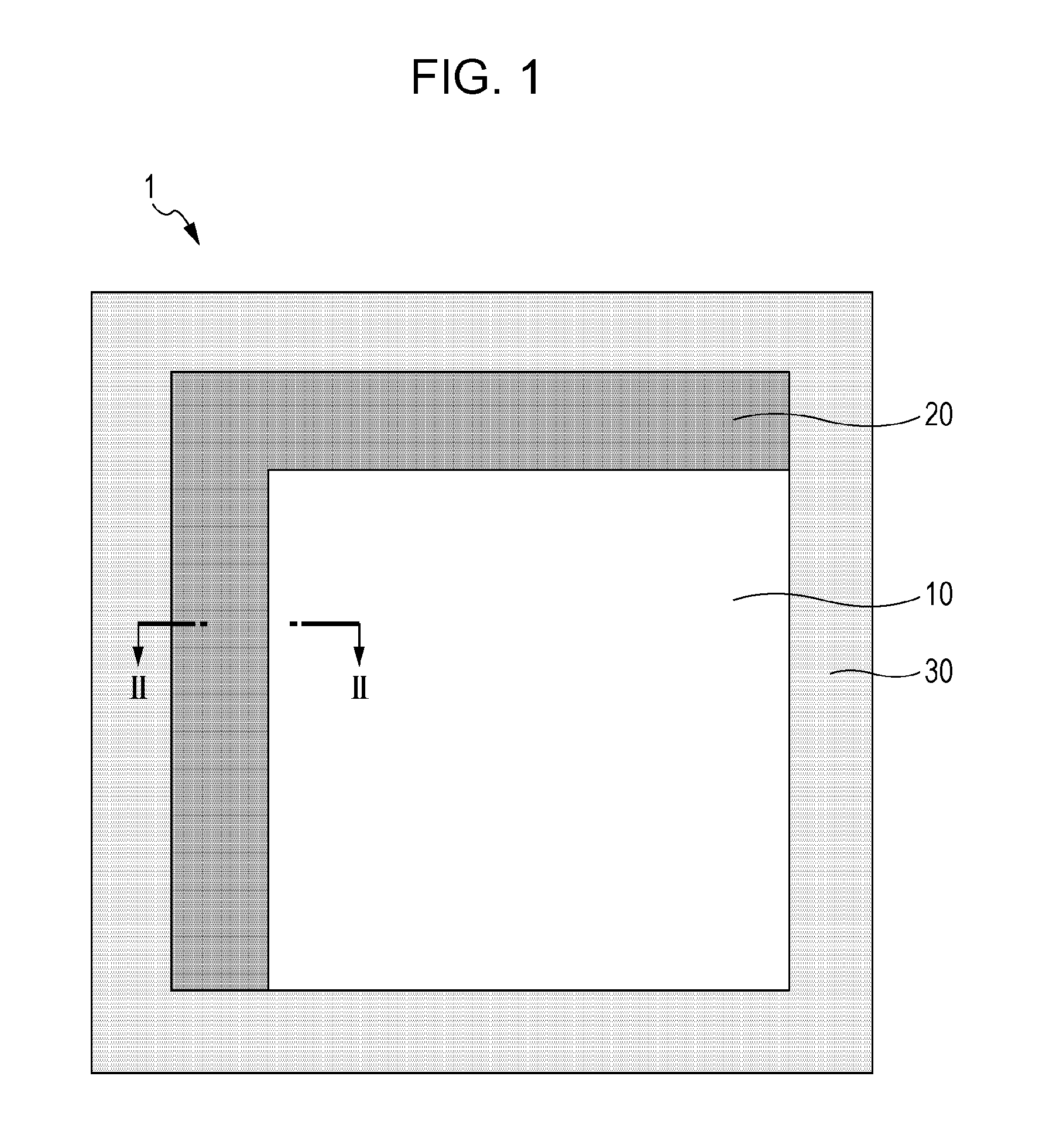
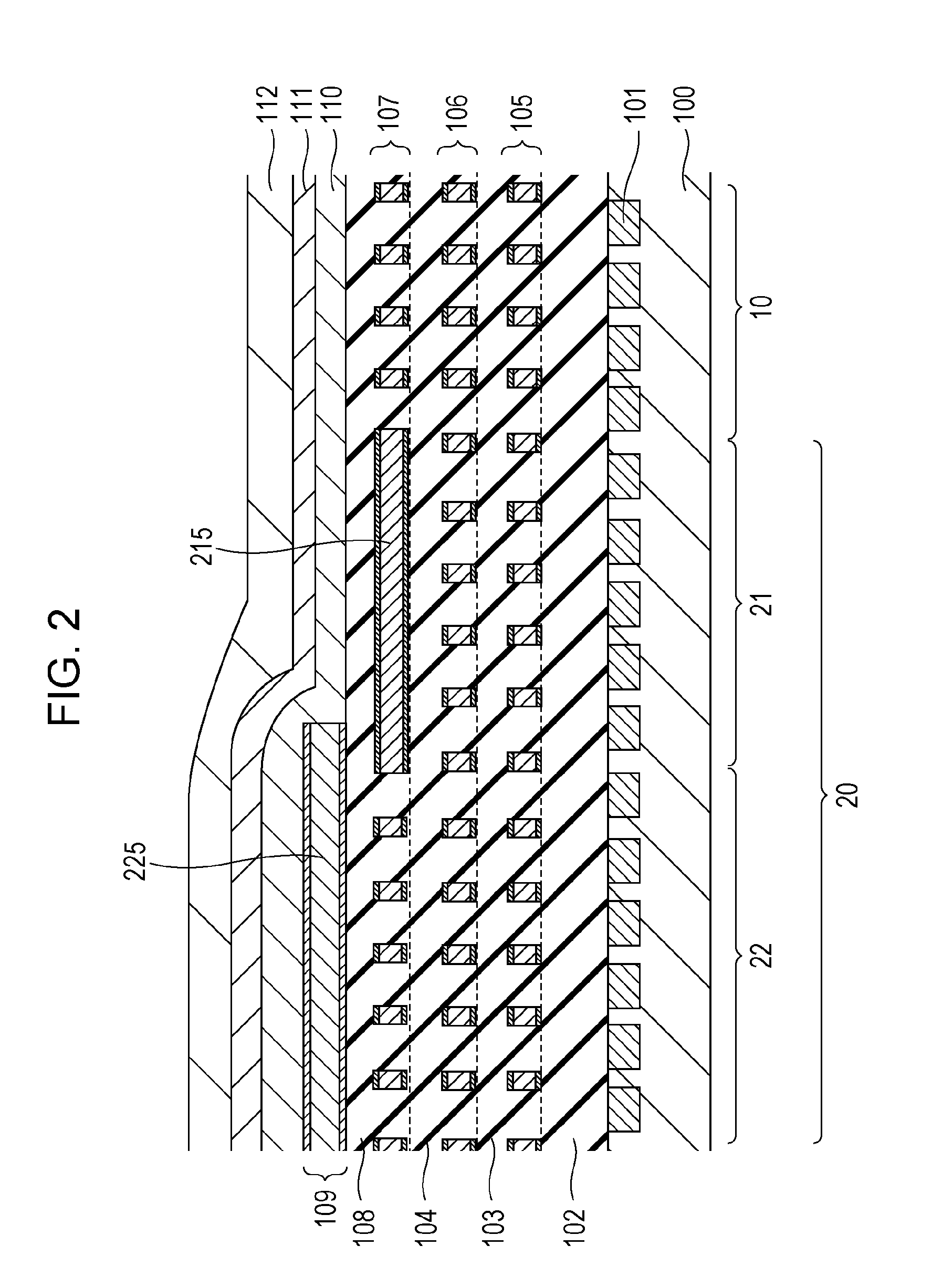
[0020]FIG. 1 is a plan layout diagram of an imaging device 1. The imaging device 1 in FIG. 1 includes a light-sensing pixel region 10, a light-shielded pixel region 20, and a peripheral circuit region 30. The light-shielded pixel region 20 is a region provided on the outer side of the light-sensing pixel region 10, and a two-dimensional array of multiple pixels is formed in the light-sensing pixel region 10 and light-shielded pixel region 20. The peripheral circuit region 30 is a region for controlling operations of the light-sensing pixel region 10 and for processing signals read from the light-sensing pixel region 10, ...

second embodiment

[0039]A second embodiment of the present invention will be described now. Structures and regions having similar functions to those in the first embodiment will be denoted with the same reference numerals, and description thereof may be omitted as appropriate.

[0040]The second embodiment according to the present invention will be described with reference to FIG. 6. The first shielding portion 215 is provided to the third wiring layer 107 and the second shielding portion 225 is provided to the fourth wiring layer 109, in the same way as with the first embodiment. The present embodiment differs from the first embodiment in that a through-hole is formed at positions where the first shielding portion 215 and second shielding portion 225 overlap in planar view. Two through-holes, TH2 and TH3, are formed between the first shielding portion 215 and second shielding portion 225. The through-hole TH2 is provided on the inner side as to the through-hole TH3, that is to say, on the light-sensing...

third embodiment

[0042]A third embodiment of the present invention will be described with reference to FIG. 8. FIG. 8 is a plan view of the present embodiment, illustrating only the third wiring layer 107 and the through-holes formed on the third wiring layer 107. Through-holes TH4 and TH5 formed between the first shielding portion 215 and second shielding portion 225 are not continuous in the plane direction, being partly discontinued in the present embodiment. However, the through-holes TH4 and TH5 are formed in an alternately continuous manner in the row direction or column direction above the boundary region between the first light-shielded pixel region 21 and the second light-shielded pixel region 22. Accordingly, the region above the second light-shielded pixel region 22 is not visible when viewed from positions above the light-sensing pixel region 10 in the third wiring layer 107.

[0043]In an arrangement where the through-holes are a continuous structure in the plane direction, as illustrated ...


PUM


Abstract

An imaging device includes a light-sensing pixel region; a first pixel region; a second pixel region; a first wiring layer disposed above the light-sensing pixel region; and a second wiring layer disposed above the topmost wiring layer of the wiring layer disposed above the light-sensing pixel region, above the second pixel region. The first pixel region is disposed between the light-sensing pixel region and the second pixel region, adjacent to the light-sensing pixel region and the second pixel region, wherein the first pixel region overlaps, in plan view, a first shielding portion included in the first wiring layer. The second pixel region overlaps, in plan view, a second shielding portion included in the second wiring layer. An electroconductive pattern is formed at the first wiring layer at a position overlapping the second pixel region in plan view.

Description

BACKGROUND OF THE INVENTION[0001]1. Field of the Invention[0002]The present invention relates to an imaging device and an imaging system, and more particularly relates to an imaging device and an imaging system having a light-sensing pixel region and a light-shielded pixel region.[0003]2. Description of the Related Art[0004]There are known imaging devices which have a light-sensing pixel region and a light-shielded pixel region. Japanese Patent Laid-Open No. 2010-267675 discloses an imaging device having a light-sensing pixel region, an invalid pixel region located on the outer side of the light-sensing pixel regions, and an optical black region (OPB region) located on the outer side of the invalid pixel region. Above the light-sensing pixel region, invalid pixel region, and OPB region, are formed wiring layers 1MT and 2MT. The wiring layers 1MT and 2MT have openings formed corresponding to photodiodes of individual pixels. Wiring layers 3MT and 4MT, which are formed further above t...

Claims


Application Information

Patent Timeline
Patent Type & Authority Applications(United States)
IPC IPC(8): H01L27/146H04N5/225H04N5/369
CPCH01L27/14623H04N5/2254H04N5/369H01L27/14636H01L27/14607H04N25/70
Inventor SUZUKI, KENTAROUTEZUKA, TOMOYUKI
Owner CANON KK
Why Eureka
Try Eureka