Supercharge Your Innovation With Domain-Expert AI Agents!

Transparent electrode layer, touch panel and electronic device

a technology of transparent electrodes and touch panels, applied in the direction of instruments, computing, electric digital data processing, etc., can solve the problems of conventional touch panels having visibility problems, non-uniform brightness distribution of images, etc., and achieve the effect of improving transmittan

Active Publication Date: 2015-07-30
INNOLUX CORP
View PDF8 Cites 13 Cited by
  • Summary
  • Abstract
  • Description
  • Claims
  • Application Information

AI Technical Summary

Benefits of technology

The present invention is related to a transparent electrode layer, a touch panel, and an electronic device with improved transparency. The invention provides a transparent electrode layer with plural touch units that have a sensing part with a dummy slit and a wiring part with alternating conductor lines and slits. The density ratio of the sensing and wiring parts is determined to be between 0.5 and 2. The invention also provides a touch panel with the transparent electrode layer and a controller for implementing a touch control procedure. The technical effects of the invention include improved transparency and touch control with high accuracy.

Problems solved by technology

In case that an image is shown on the touch panel, the arrangement of the transparent electrodes 12 may result in non-uniform brightness distribution of the image.
In other words, the conventional touch panel has a visibility issue.

Method used


Image

  • Transparent electrode layer, touch panel and electronic device
  • Transparent electrode layer, touch panel and electronic device
  • Transparent electrode layer, touch panel and electronic device

Examples


Embodiment Construction

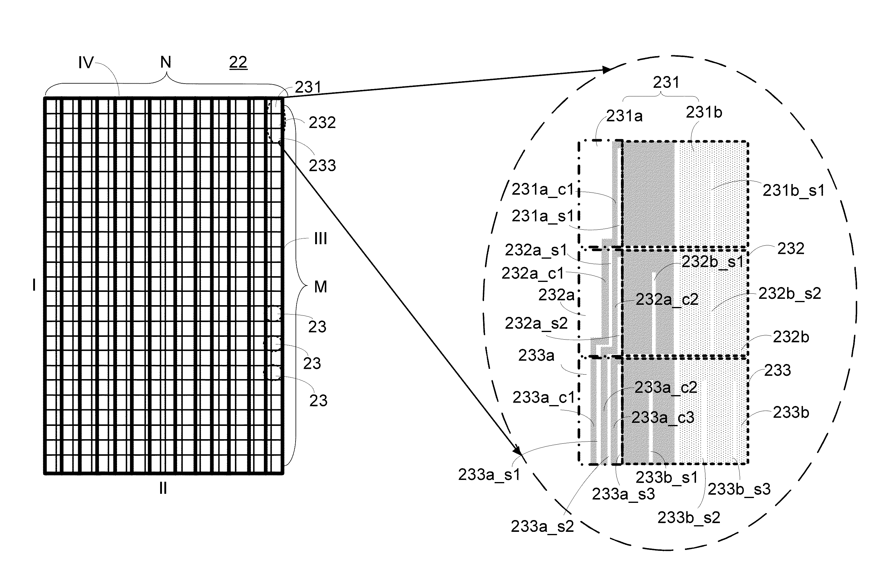
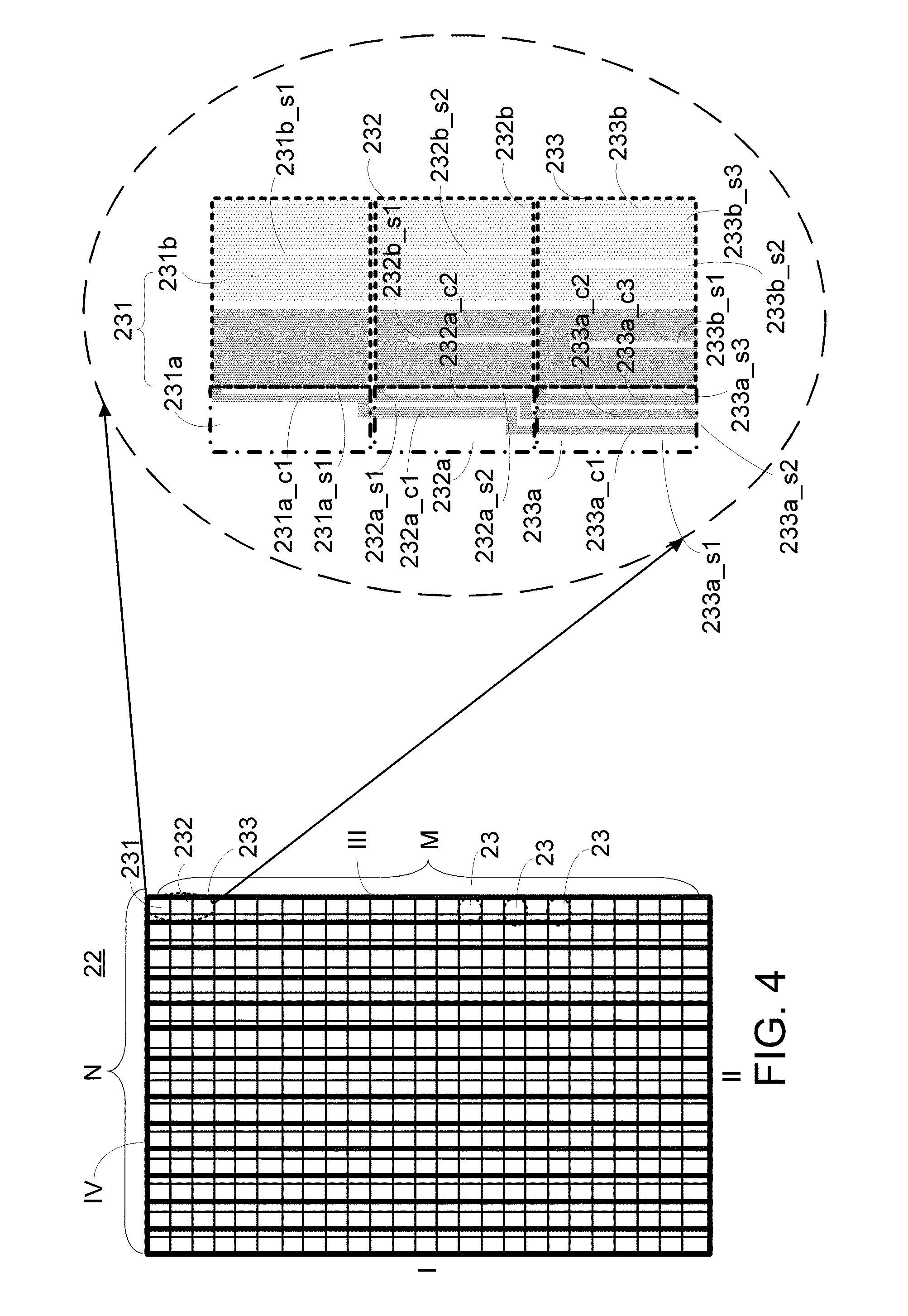
[0029]As previously described, the transmittance of the locations corresponding to the transparent electrodes is lower than the transmittance of the other locations of the touch panel. That is, the arrangement of the transparent electrodes may result in non-uniform brightness distribution of the image. For solving the drawbacks, the present invention provides a transparent electrode layer, a touch panel and an electronic device. The touch panel includes a display layer and the transparent electrode layer. The transparent electrode layer is disposed above the display layer. For example, the display layer is a liquid crystal layer, an electro-phoretic display (EPD) layer or a cholesteric liquid crystal display (CLCD) layer. The transparent electrode layer includes plural touch units. Each touch unit includes a wiring part and a sensing part. Moreover, plural dummy slits are formed in the sensing part. Due to the dummy slits, the contrast of the touch panel is reduced. Since the contra...


PUM


Abstract

A transparent electrode layer includes plural touch units. Each of the touch units includes a sensing part and a wiring part. The sensing part has at least one dummy slit. The wiring part is electrically connected to the sensing part, and includes at least one conductor line and at least one slit. The at least one conductor line and the at least one slit are alternately formed in the wiring part. A density ratio, in a range between 0.5 and 2, is determined by a sensing part density parameter and a wiring part density parameter.

Description

[0001]This application claims the benefit of U.S. provisional application Ser. No. 61 / 930,990, filed Jan. 24, 2014, the subject matter of which is incorporated herein by reference.FIELD OF THE INVENTION[0002]The present invention relates to a transparent electrode layer, a touch panel and an electronic device, and more particularly to a transparent electrode layer, a touch panel and an electronic device with dummy slits.BACKGROUND OF THE INVENTION[0003]Generally, a touch panel has both a displaying function and a touch control function. The touch control function may be implemented according to a resistive sensing technology, a capacitive sensing technology or an infrared sensing technology etc.[0004]FIG. 1 is a schematic side view illustrating a conventional touch panel. As shown in FIG. 1, from bottom to top, the touch panel 1 includes a lower polarizer 18, a thin film transistor (hereinafter, TFT) substrate 19, a liquid crystal layer 17, a color film substrate 15, an upper polari...

Claims


Application Information

Patent Timeline
IPC IPC(8): G06F3/047G06F3/041
CPCG06F3/047G06F3/0416G06F3/0412G06F3/0443G06F3/045G06F2203/04103
Inventor NAITO, SHUSAKUCHEN, JIAN-CHENGMORI, AYUMUEDO, KEIKOHSIEH, HONG-SHENG
Owner INNOLUX CORP
Features
  • R&D
  • Intellectual Property
  • Life Sciences
  • Materials
  • Tech Scout
  • Unparalleled Data Quality
  • Higher Quality Content
  • 60% Fewer Hallucinations
Learn More