Organic light emitting display device and method of manufacturing the same

a technology of light-emitting display device and organic light-emitting display device, which is applied in the field of display device, can solve the problems of increasing power consumption and occurrence of color abnormality phenomenon, and achieve the effect of reducing contact resistance and stably providing

Active Publication Date: 2015-08-13
SAMSUNG DISPLAY CO LTD
View PDF6 Cites 105 Cited by
  • Summary
  • Abstract
  • Description
  • Claims
  • Application Information

AI Technical Summary

Benefits of technology

[0029]Therefore, an organic light emitting display (OLED) device and a method of manufacturing the OLED device according to example embodiments may decrease a contact resistance by forming ...

Problems solved by technology

When the contact area in which the organic light emitting elements and the power supply line are coupled is decreased, a cont...

Method used


Image

  • Organic light emitting display device and method of manufacturing the same
  • Organic light emitting display device and method of manufacturing the same
  • Organic light emitting display device and method of manufacturing the same

Examples


Embodiment Construction

[0042]Hereinafter, the present inventive concept will be explained in detail with reference to the accompanying drawings.

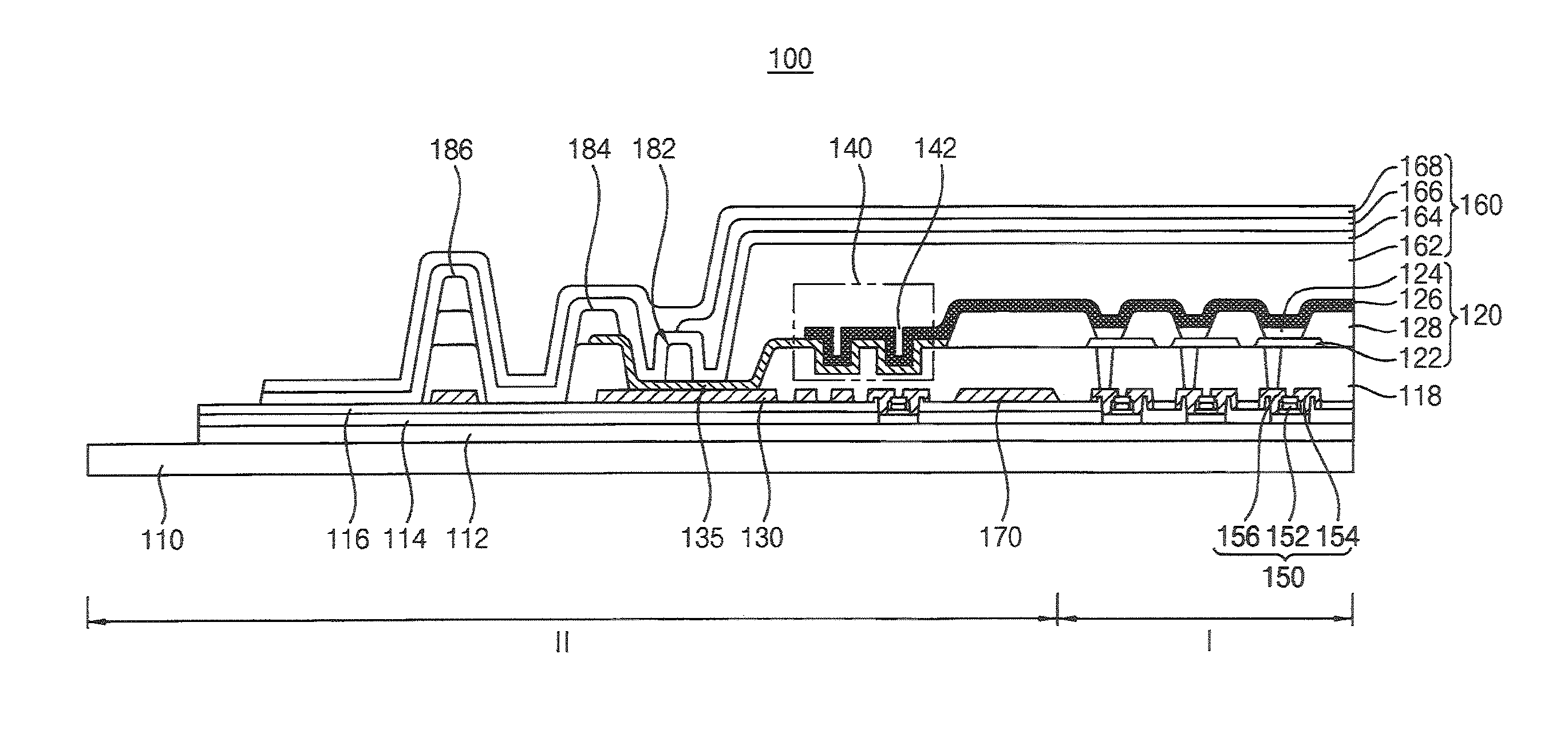
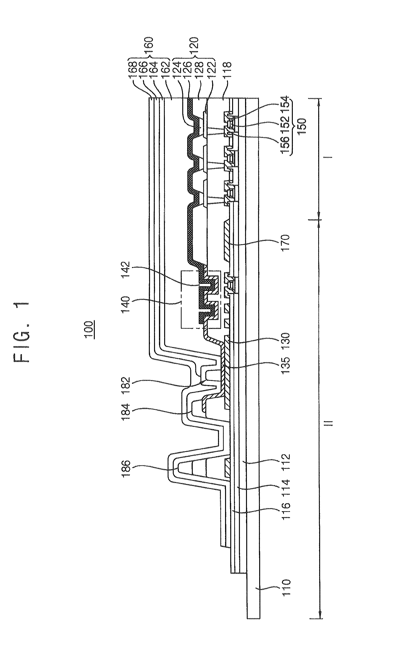
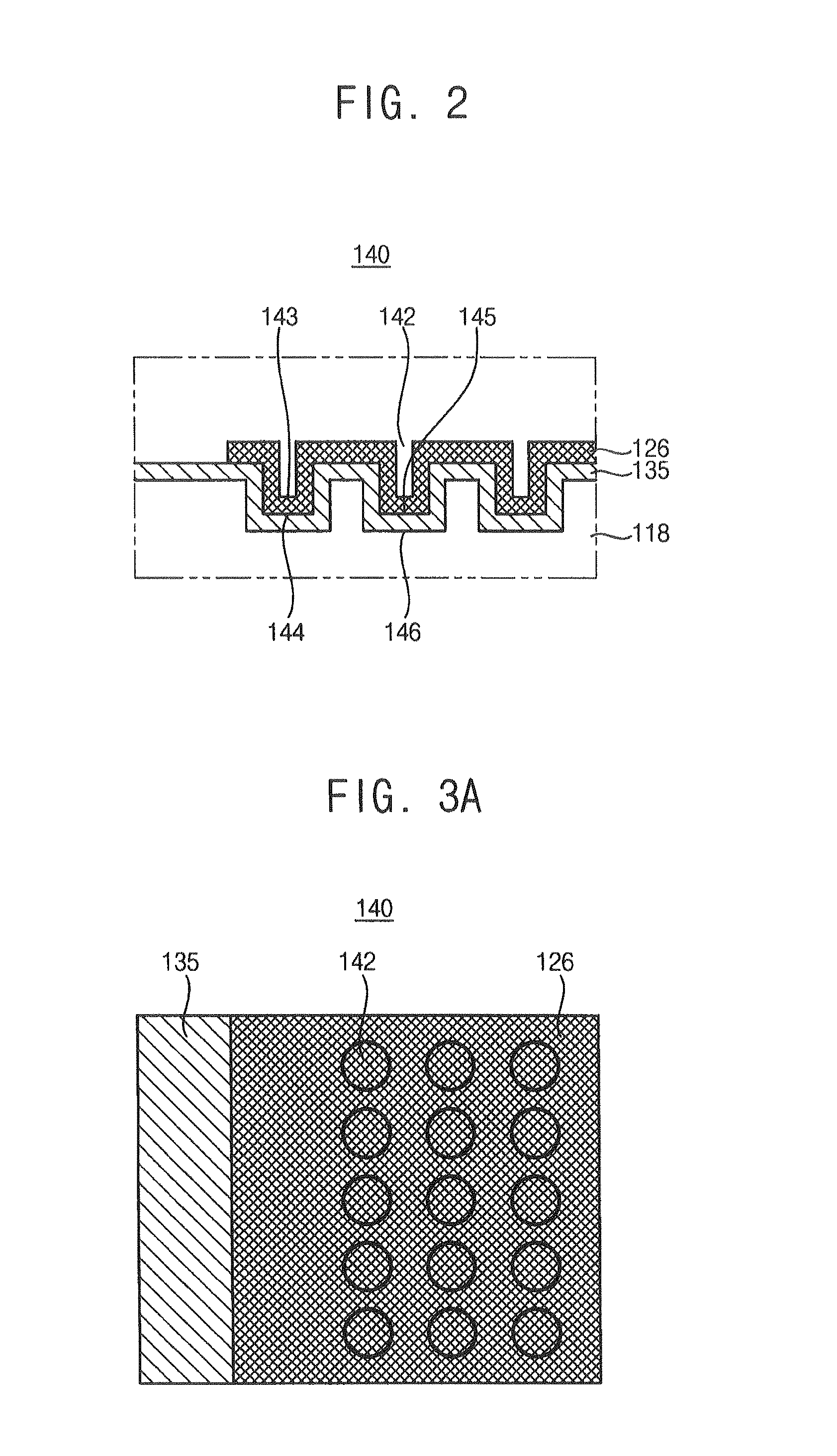
[0043]FIG. 1 is a cross-sectional view illustrating an organic light emitting display (OLED) device according to example embodiments and FIG. 2 is a cross-sectional view illustrating a contact region that is included in the OLED device of FIG. 1.

[0044]FIG. 1 is a cross-sectional view illustrating a pixel that is disposed in an outside of an organic light emitting display (OLED) device 100. In reference to FIG. 1, the OLED device may include a substrate 110, a plurality of light emitting structures 120, a power supply line 130, a third electrode 135, and an encapsulation member 160. The substrate 110 of the OLED device 100 may include a display region I and a peripheral region II. In an embodiment, the display region I displays the information of images or characters and the peripheral region II does not display the information and the peripheral region II surround...


PUM


Abstract

An organic light emitting display (OLED) device includes a substrate, a plurality of first electrodes, a plurality of light emitting layers, a second electrode, a power supply line, a third electrode, and an encapsulation member. The third electrode that is formed on the power supply line and the second electrode that is formed on the light emitting layers extend to a contact region that is in a peripheral region of the substrate. The third electrode and the second electrodes have an uneven pattern in the contact region.

Description

CLAIM OF PRIORITY[0001]This application makes reference to, incorporates the same herein, and claims all benefits accruing under 35 U.S.C. §119 from an application earlier filed in the Korean Intellectual Property Office on 12 Feb. 2014 and there duly assigned Serial No. 10-2014-0015892.BACKGROUND OF THE INVENTION[0002]1. Field of the Invention[0003]Example embodiments of the present invention relate generally to a display device. More particularly, embodiments of the present invention relate to an organic light emitting display device and a method of manufacturing the organic light emitting display device.[0004]2. Description of the Related Art[0005]An organic light emitting display (OLED) device displays information of images or characters by using light generated when holes and electrons that are provided from an anode and a cathode, respectively are combined with each other at an organic light emitting layer interposed between the anode and the cathode. The OLED device has been ...

Claims


Application Information

Patent Timeline
IPC IPC(8): H01L51/52H01L51/56
CPCH01L51/5256H01L51/5225H01L51/5209H01L51/56H10K59/124H10K59/122H10K59/131H10K50/8445H10K50/8426H10K59/805H10K50/805H10K50/85H10K50/813H10K50/822H10K71/00
Inventor KIM, YONG-JIN
Owner SAMSUNG DISPLAY CO LTD
Why Eureka
Try Eureka