This helps you quickly interpret patents by identifying the three key elements:
Problems solved by technology
Method used
Benefits of technology
Benefits of technology
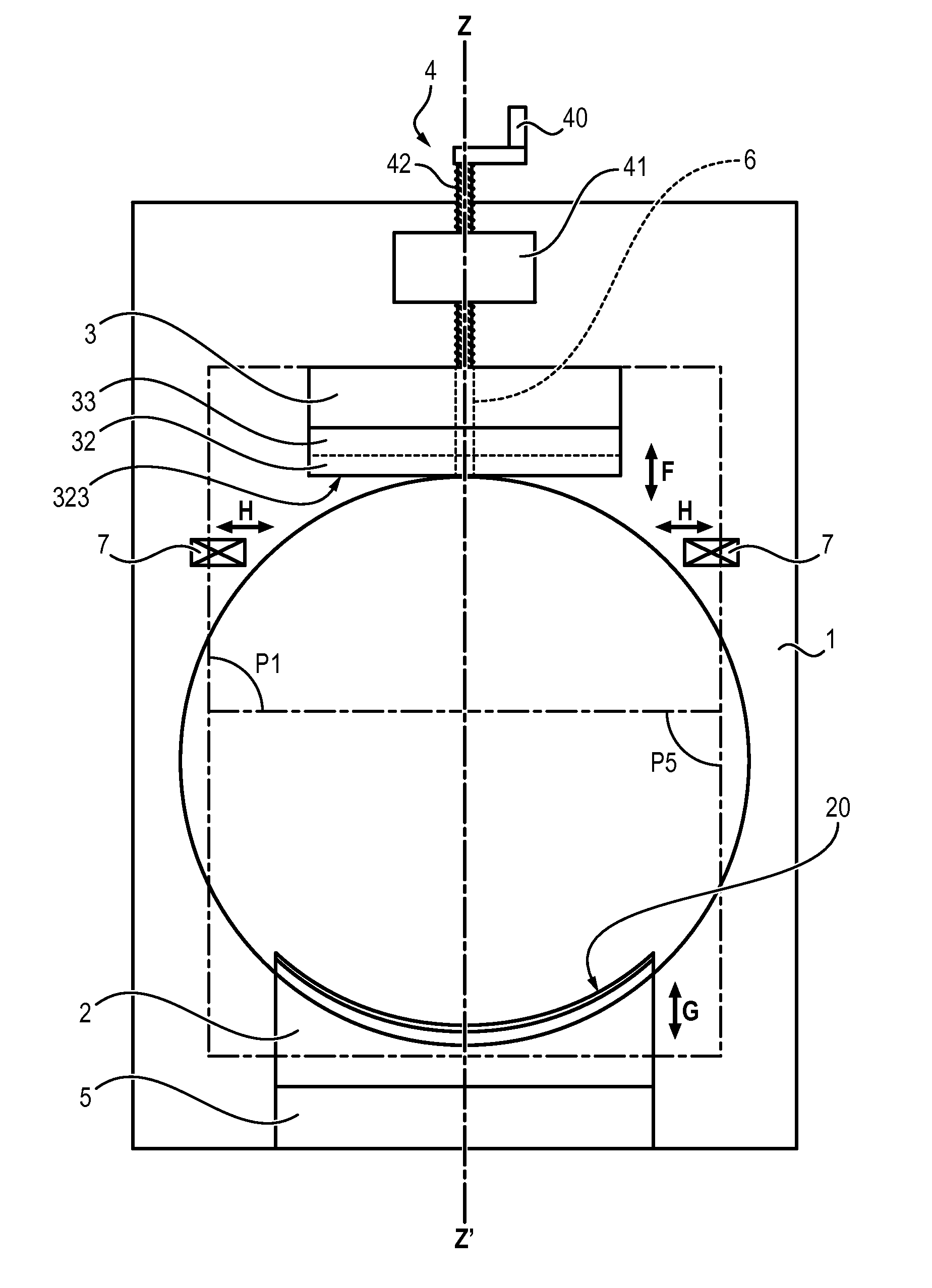
The technical effect of this patent text is to provide a device that can detach two large substrates or layers without scratching, contaminating, breaking, or accidentally rebonding them. The device has moving means to move the separating tool and retaining member closer or farther apart from each other, which are preferably limited in their travel.
Problems solved by technology
Furthermore, the larger the size of the two substrates of the structure to be separated or the higher their separation energy (i.e., the energy required to separate them), the more difficult it is to separate them, especially without damage.
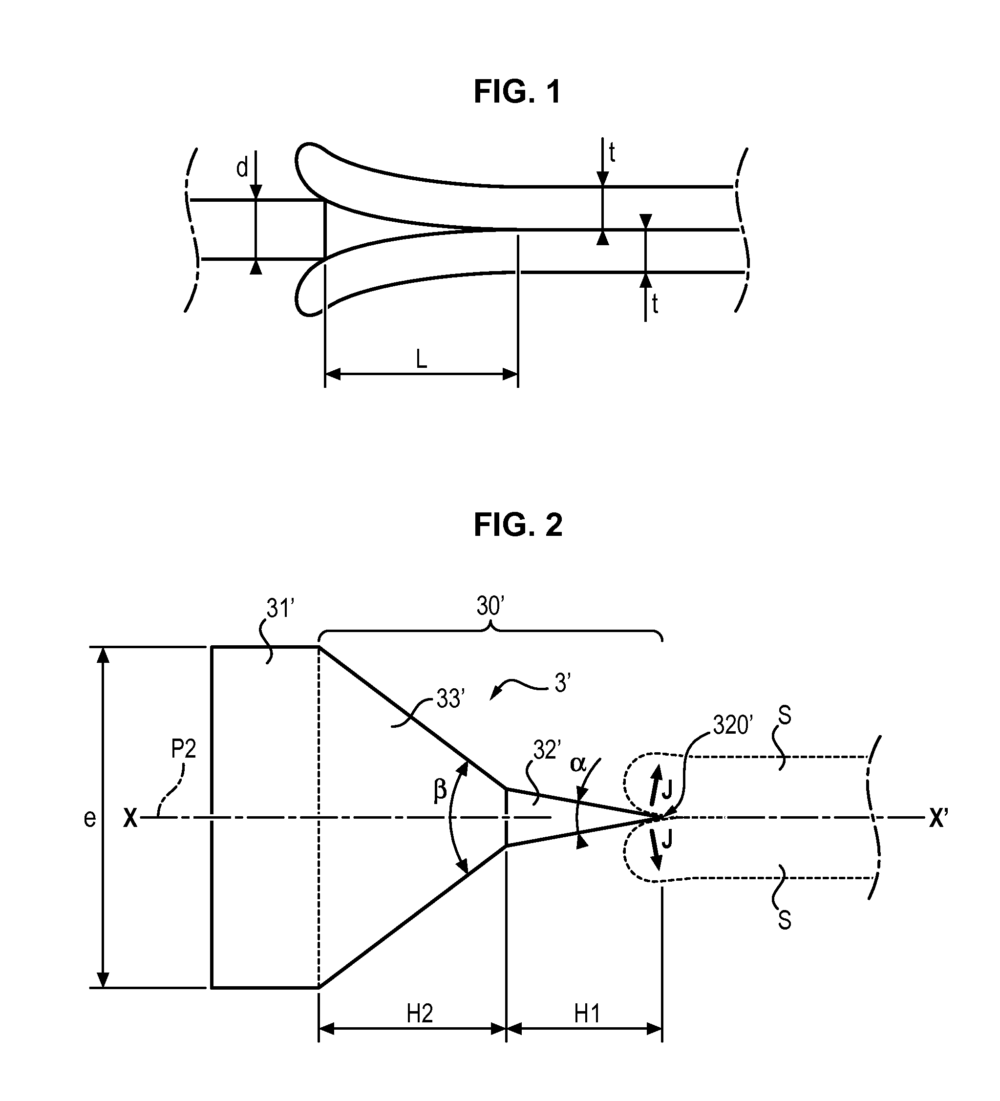
Thus, the blade used is thin (between 0.05 mm and 0.5 mm in thickness) and risks scratching the bonded sides of the two substrates.
However, such a technique is not envisaged when it is desired to reuse the substrates.
This device has the drawback that, once the two wafers have been separated, they are not supported and risk being damaged or bonding to each other again.
However, U.S. Pat. No. 7,406,994 provides no teaching on the possibility of separating substrates of large diameter or having a large bonding energy, for example, at least 1 J / m2, even 1.5 J / m2.
Such a thin blade does not allow this to be done because it does not allow the substrates to be sufficiently parted.
Furthermore, the risk of scratching the surfaces with such a blade is not negligible.
It is, therefore, difficult to part the two substrates from each other.
Method used
Image
Click on the blue label to locate the original text in one second.
Reading with bidirectional positioning of images and text.
Examples
first embodiment
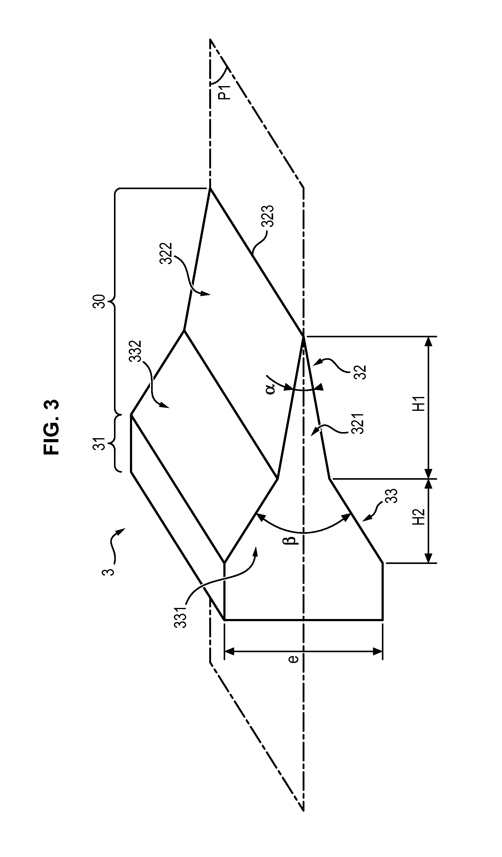
[0070]the separating tool 3 will now be described with reference to FIG. 3.
[0071]The separating tool 3 comprises a front portion 30 or “leading edge” that is extended by a back portion 31.
[0072]The back portion 31 preferably has the shape of a rectangular parallelepiped and serves for fastening to the holder 1.
[0073]The leading edge 30 itself comprises, in succession from front to back (i.e., from right to left in FIG. 3), a tapered portion 32 and a flared portion 33.
[0074]The tapered portion 32 has the shape of a triangular prism, the base of which is an isosceles triangle. The two isosceles triangle-shaped end faces are referenced 321, whereas the two longitudinal rectangular faces located in the extension of the sides of the same length of the two isosceles triangles 321 are referenced 322. The free edge or front edge of the prism, located at the junction of the two faces 322, has been given the reference 323.
[0075]The angle α between the two lateral faces 322, designated the “an...
second embodiment
[0088]the separating tool (referenced 3″) will now be described with regard to FIG. 5.
[0089]It differs from the tool 3 in that its leading edge 30″ has the general shape of a prism, the base of which has the shape of an isosceles triangle but the two equal sides of which are concave. The back portion 31″ preferably has the shape of a rectangular parallelepiped.
[0090]The two end faces are referenced 301″, the two concave faces 302″ and the edge that joins them 303″.
[0091]Also, preferably, each face 302″ has the profile of a half parabola, the tip of the parabola being located level with the intersection of the back portion 31″.
[0092]The leading edge 30″, therefore, again has a tapered portion 32″ and a flared portion 33″, but its gradient does not change abruptly. Furthermore, it has the general shape of an elongate rectilinear element.
[0093]The height H3 of the face 301″ is preferably between 10 mm and 120 mm and, even more preferably, is equal to 60 mm. Its thickness e1 is preferab...
PUM
Abstract
This disclosure relates to a device for separating two substrates to be utilized in electronics, optics, optoelectronics and / or photovoltaics. The device separates the substrates at an interface, the device comprising:a holder;a member for retaining the structure, the member being mounted on the holder;a tool for separating the two substrates, also mounted on the holder; andmeans for moving the separating tool and / or means for moving the retaining member relative to the holder so as to bring them closer together or move them farther apart from each other, preferably over a limited range of travel.This device is noteworthy in that the separating tool comprises a leading edge that has, in cross-section, in succession from its tip or its front edge to its back, a tapered portion that is extended by a flared portion.
Description
CROSS-REFERENCE TO RELATED APPLICATIONS[0001]This application is a national phase entry under 35 U.S.C. §371 of International Patent Application PCT / IB2013 / 001921, filed Sep. 3, 2013, designating the United States of America and published as International Patent Publication WO 2014 / 037791 A1 on Mar. 13, 2014, which claims the benefit under Article 8 of the Patent Cooperation Treaty and under 35 U.S.C. §119(e) to French Patent Application Serial No. 1258370, filed Sep. 7, 2012, the disclosure of each of which is hereby incorporated herein in its entirety by this reference.TECHNICAL FIELD[0002]The disclosure relates to a device for separating two substrates at a “separation” interface, at least one of these two substrates being intended to be used in electronics, optics, optoelectronics and / or photovoltaics, these two substrates together forming a structure.BACKGROUND[0003]This mechanical separation may be carried out along various types of separation interfaces.[0004]A first type of ...
Claims
Application Information
Patent Timeline
Application Date:The date an application was filed.
Publication Date:The date a patent or application was officially published.
First Publication Date:The earliest publication date of a patent with the same application number.
Issue Date:Publication date of the patent grant document.
PCT Entry Date:The Entry date of PCT National Phase.
Estimated Expiry Date:The statutory expiry date of a patent right according to the Patent Law, and it is the longest term of protection that the patent right can achieve without the termination of the patent right due to other reasons(Term extension factor has been taken into account ).
Invalid Date:Actual expiry date is based on effective date or publication date of legal transaction data of invalid patent.

