Semiconductor device, display device including the semiconductor device, display module including the display device, and electronic appliance including the semiconductor device, the display device, and the display module
a semiconductor device and display module technology, applied in semiconductor devices, electrical appliances, instruments, etc., can solve the problems of electrical characteristics fluctuation among transistors, affecting transistor characteristics, etc., and achieve the effect of improving reliability and low power consumption
- Summary
- Abstract
- Description
- Claims
- Application Information
AI Technical Summary
Benefits of technology
Problems solved by technology
Method used
Image

Examples
embodiment 1
[0084]In this embodiment, a semiconductor device of one embodiment of the present invention is described with reference to FIGS. 1A to 1C, FIGS. 2A to 2D, FIGS. 3A to 3C, FIGS. 4A to 4D, FIGS. 5A to 5C, FIGS. 6A to 6D, FIGS. 7A to 7C, FIGS. 8A to 8D, FIGS. 9A and 9B, FIGS. 10A to 10D, FIGS. 11A to 11D, FIGS. 12A to 12D, FIGS. 13A and 13B, FIGS. 14A to 14D, FIGS. 15A to 15D, FIGS. 16A to 16D, FIGS. 17A to 17D, and FIGS. 18A to 18C.
Structural Example 1 of Semiconductor Device
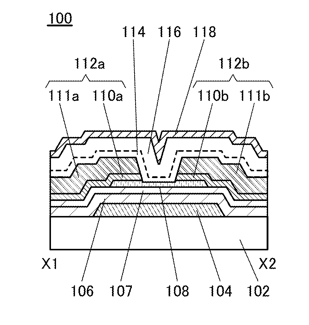
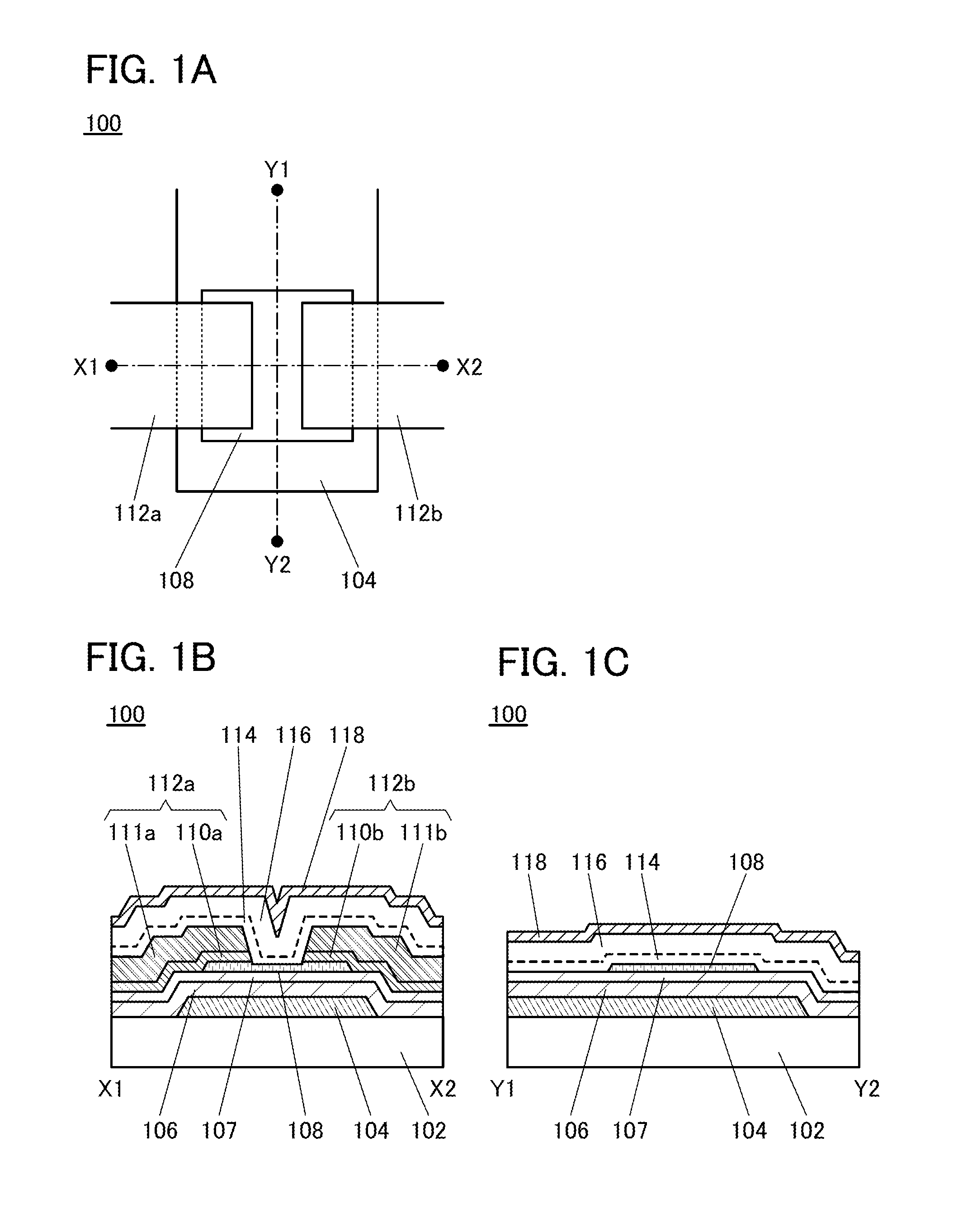
[0085]FIG. 1A is a top view of a transistor 100 that is a semiconductor device of one embodiment of the present invention. FIG. 1B is a cross-sectional view taken along a dashed dotted line X1-X2 in FIG. 1A, and FIG. 1C is a cross-sectional view taken along a dashed dotted line Y1-Y2 in FIG. 1A. Note that in FIG. 1A, some components of the transistor 100 (e.g., an insulating film serving as a gate insulating film) are not illustrated to avoid complexity. Furthermore, the direction of the dashed dotted line X1-X1 m...
example 4
Structure Example 4 of Semiconductor Device
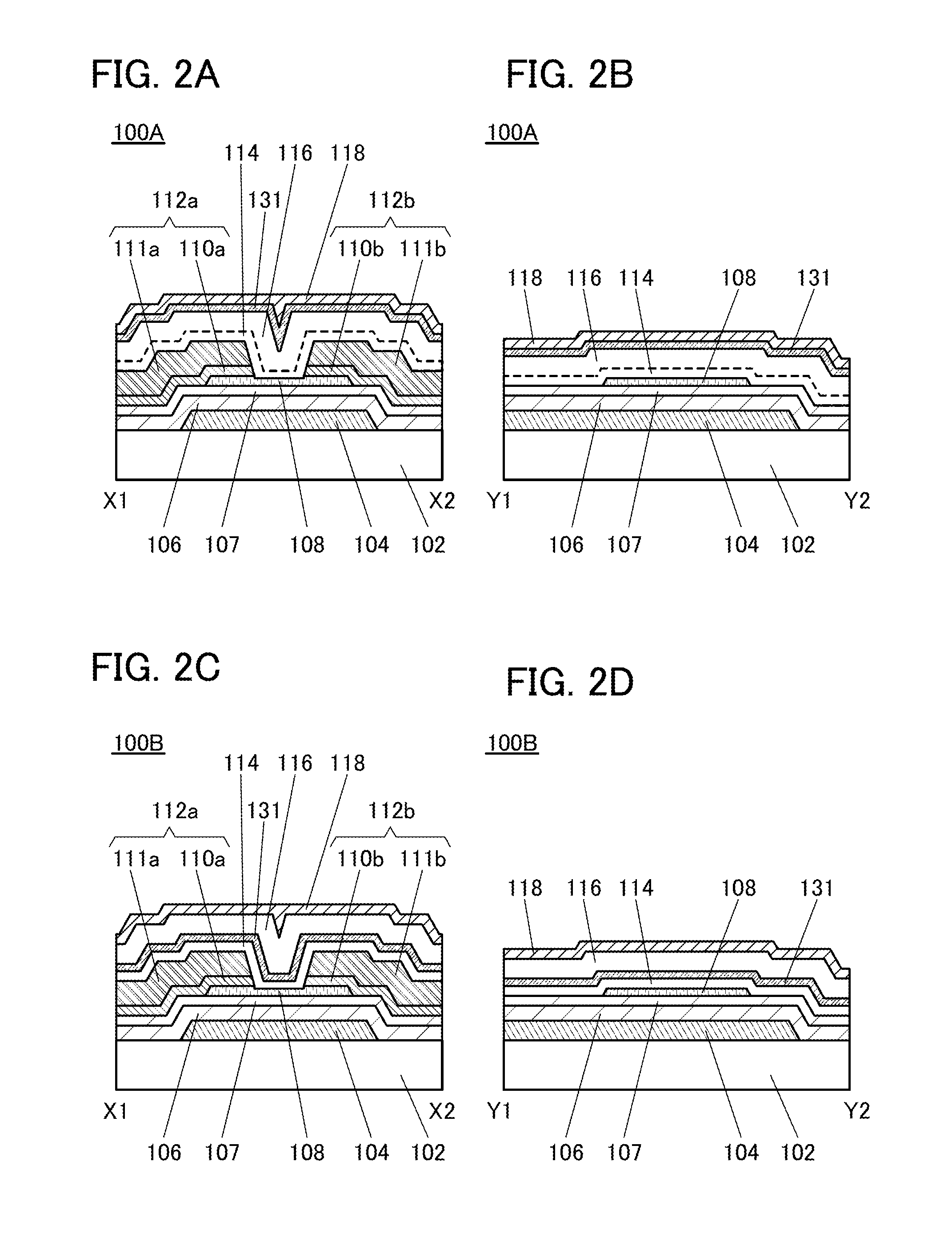
[0165]FIG. 4A is a cross-sectional view in the channel length direction of a transistor 150A and FIG. 4B is a cross-sectional view in the channel width direction of the transistor 150A. FIG. 4C is a cross-sectional view in the channel length direction of a transistor 150B and FIG. 4D is a cross-sectional view in the channel width direction of the transistor 150B. Note that top views of the transistor 150A and the transistor 150B are omitted here because they are similar to the top view of FIG. 3A.
[0166]The transistor 150A illustrated in FIGS. 4A and 4B includes the conductive film 104 functioning as a gate electrode over the substrate 102, the insulating film 106 over the substrate 102 and the conductive film 104, the insulating film 107 over the insulating film 106, the oxide semiconductor film 108 over the insulating film 107, the insulating film 114 over the oxide semiconductor film 108, the insulating film 116 over the insulating film 1...
example 5
Structural Example 5 of Semiconductor Device
[0171]FIG. 5A is a top view of a transistor 160 that is a semiconductor device of one embodiment of the present invention. FIG. 5B is a cross-sectional view taken along a dashed dotted line X1-X2 in FIG. 5A, and FIG. 5C is a cross-sectional view taken along a dashed dotted line Y1-Y2 in FIG. 5A.
[0172]The transistor 160 includes the conductive film 104 functioning as a gate electrode over the substrate 102, the insulating film 106 over the substrate 102 and the conductive film 104, the insulating film 107 over the insulating film 106, the oxide semiconductor film 108 over the insulating film 107, the insulating film 114 over the oxide semiconductor film 108, the insulating film 116 over the insulating film 114, and the conductive films 112a and 112b functioning as source and drain electrodes electrically connected to the oxide semiconductor film 108. Over the transistor 160, specifically, over the conductive films 112a and 112b and the insu...
PUM
 Abstract
Description
Claims
Application Information
 - R&D Engineer
- R&D Manager
- IP Professional
- Industry Leading Data Capabilities
- Powerful AI technology
- Patent DNA Extraction
Browse by: Latest US Patents, China's latest patents, Technical Efficacy Thesaurus, Application Domain, Technology Topic.
© 2024 PatSnap. All rights reserved.Legal|Privacy policy|Modern Slavery Act Transparency Statement|Sitemap