Semiconductor device with reduced warpage

a technology of semiconductor devices and warpage, which is applied in the direction of semiconductor devices, semiconductor/solid-state device details, electrical equipment, etc., can solve the problems of severe defects in the operation of semiconductor devices, warpage of semiconductor packages, and lower reliability of semiconductor packages, so as to reduce warpage

Inactive Publication Date: 2015-09-10
AMKOR TECH INC
View PDF8 Cites 42 Cited by
  • Summary
  • Abstract
  • Description
  • Claims
  • Application Information

AI Technical Summary

Problems solved by technology

However, warpage may occur to a semiconductor package due to a difference between coefficients of thermal expansion between silicon forming a semiconductor die and an underfill material underfilling the semiconductor die.
The warpage may lower reliability of the semiconductor package and may cause severe defects to the operation of a semiconductor device.

Method used


Image

  • Semiconductor device with reduced warpage
  • Semiconductor device with reduced warpage
  • Semiconductor device with reduced warpage

Examples


Embodiment Construction

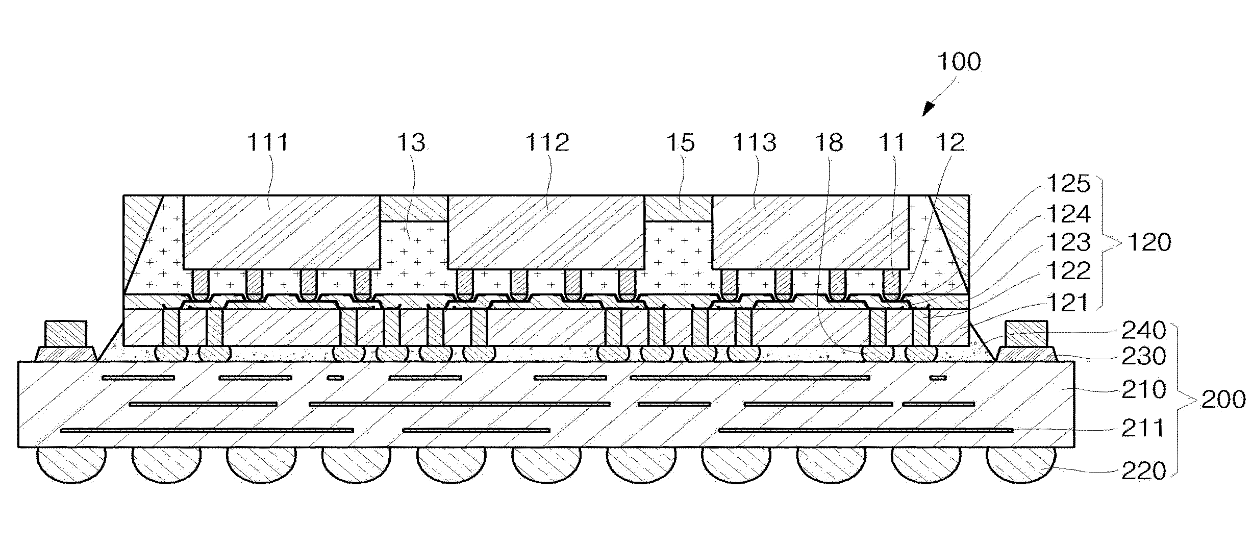
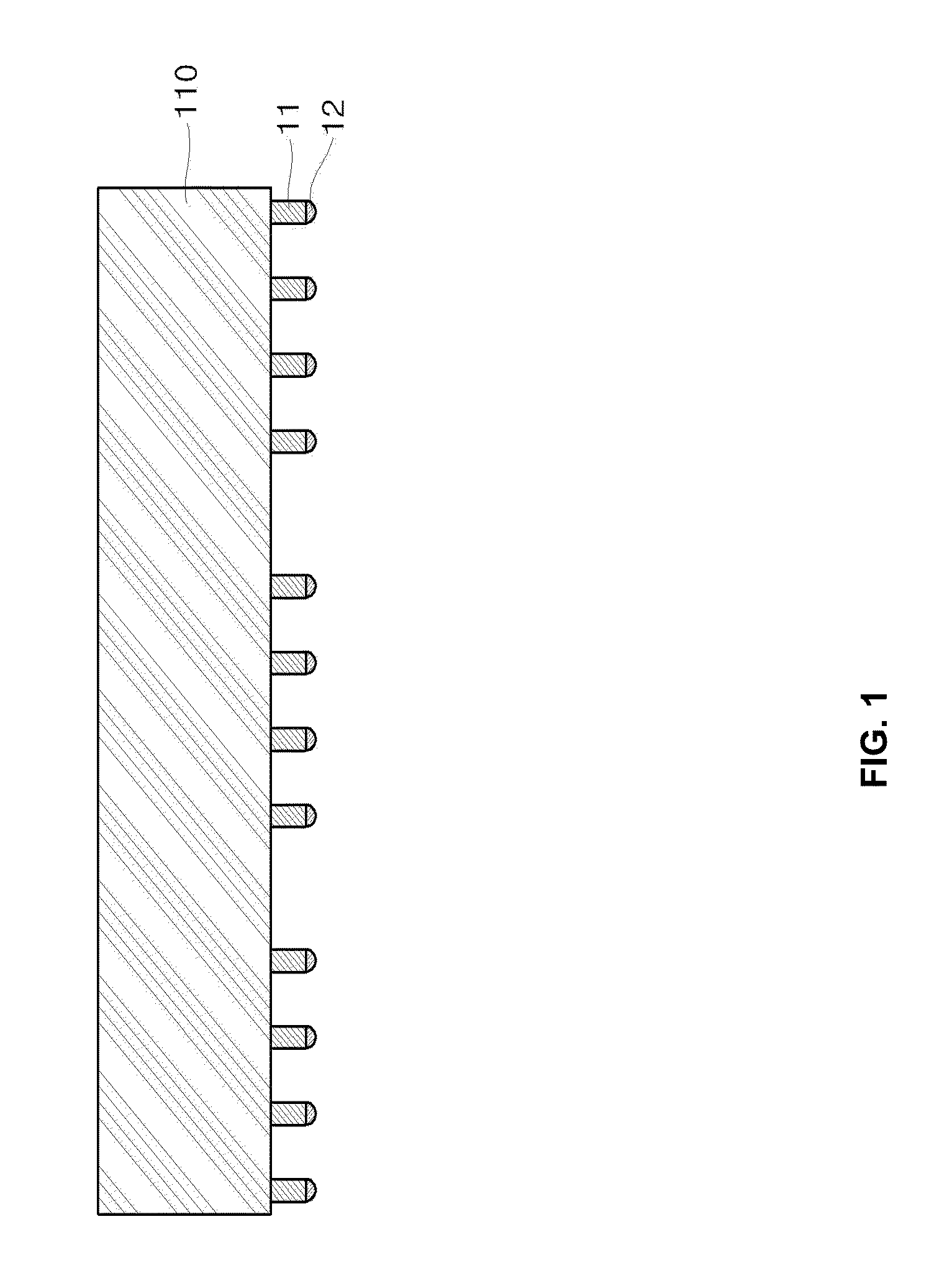
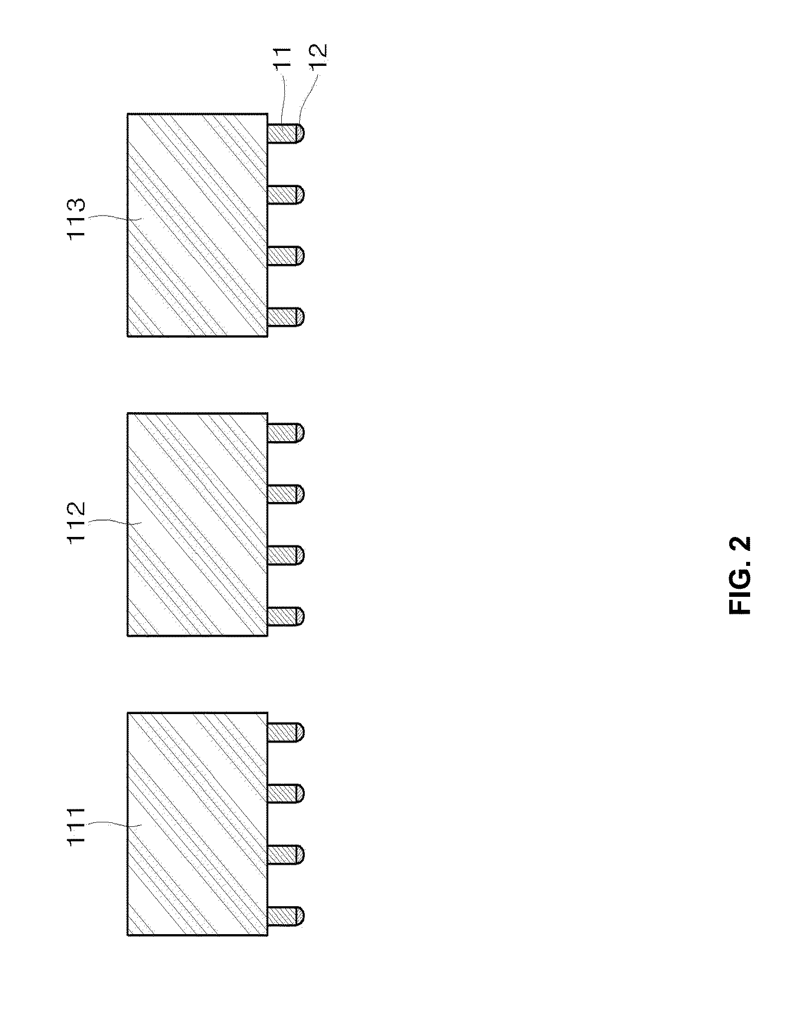
[0012]Certain aspects of the disclosure may be found in method for manufacturing a semiconductor device comprising bonding at least two semiconductor die to a substrate, forming underfill material between the at least two semiconductor die and the substrate and between the at least two semiconductor die, and removing a portion of the underfill material between the at least two semiconductor die, thereby forming a groove. The at least two semiconductor die and the underfill material may be encapsulated utilizing an encapsulant. The groove may be filled using the encapsulant. The underfill material between the at least two semiconductor die may be removed utilizing laser etching. The portion of the underfill material between the at least two semiconductor die may be removed to a depth of 60-70% of a thickness of the at least two semiconductor die. The substrate may be grinded to expose a through electrode. A solder ball may be formed on the exposed through electrode. The substrate may...


PUM


Abstract

A semiconductor device with reduced warpage is disclosed and may, for example, include bonding at least two semiconductor die to a substrate, forming underfill material between the at least two semiconductor die and the substrate and between the at least two semiconductor die, and removing a portion of the underfill material between the at least two semiconductor die, thereby forming a groove. The at least two semiconductor die and the underfill material may, for example, be encapsulating utilizing an encapsulant. The groove may, for example, be filled using the encapsulant. The underfill material between the at least two semiconductor die may, for example, be removed utilizing laser etching. The underfill material between the at least two semiconductor die may, for example, be removed to a depth of 60-70% of a thickness of the at least two semiconductor die.

Description

CROSS-REFERENCE TO RELATED APPLICATIONS[0001]The present application makes reference to, claims priority to, and claims the benefit of Korean Patent Application No. 10-2014-0025630, filed on Mar. 4, 2014, the contents of which are hereby incorporated herein by reference, in their entirety.FIELD[0002]Certain embodiments of the disclosure relate to semiconductor chip packaging. More specifically, certain embodiments of the disclosure relate to a semiconductor device with reduced warpage.BACKGROUND[0003]In general, a semiconductor package includes a semiconductor die, a plurality of leads electrically connected to the semiconductor die and an encapsulant encapsulating the semiconductor die and the leads.[0004]Along with the tendency toward miniaturization of electronic products, the electronic products need to have high performance. Accordingly, research and development of various techniques for providing high-capacity semiconductor packages are under way. One of the techniques for pro...

Claims


Application Information

Patent Timeline
Patent Type & Authority Applications(United States)
IPC IPC(8): H01L23/00H01L25/065H01L23/48H01L21/78H01L21/56H01L21/768H01L25/00H01L23/31
CPCH01L24/96H01L25/50H01L25/0655H01L23/3178H01L21/78H01L21/561H01L2224/81801H01L24/81H01L24/17H01L21/76898H01L23/481H01L23/562H01L2224/16227H01L21/563H01L21/6835H01L2221/68327H01L2221/6834H01L2224/13082H01L2224/131H01L2224/13147H01L2224/16235H01L2224/32225H01L2224/73204H01L2224/81439H01L2224/81444H01L2224/81447H01L2224/81455H01L2224/92125H01L2224/94H01L2224/97H01L2924/15311H01L2924/157H01L2924/15788H01L2924/1815H01L2924/18161H01L2924/19105H01L2924/3511H01L2924/12042H01L21/56H01L23/3135H01L2224/16237H01L23/147H01L21/486H01L23/5384H01L23/5385H01L2224/13023H01L2224/81H01L2224/11H01L2924/014H01L2924/00H01L2924/00014H01L2224/16225
Inventor SON, SEUNG NAMSUNG, PIL JEDO, WON CHULLEE, JUNGBAELEE, JI HUN
Owner AMKOR TECH INC
Why Eureka
Try Eureka