Method for driving semiconductor device

Active Publication Date: 2015-09-10
SEMICON ENERGY LAB CO LTD
View PDF6 Cites 9 Cited by
  • Summary
  • Abstract
  • Description
  • Claims
  • Application Information

AI Technical Summary

Benefits of technology

This patent aims to provide a novel circuit configuration that can change the frequency of oscillation or achieve this change. This circuit configuration can exist as a semiconductor device and has the ability to switch between different frequencies. This technology allows for more flexibility and versatility in semiconductor devices.

Problems solved by technology

Conventional PLL circuits have difficulty changing oscillation frequencies instantly.

Method used


Image

  • Method for driving semiconductor device
  • Method for driving semiconductor device
  • Method for driving semiconductor device

Examples


embodiment 1

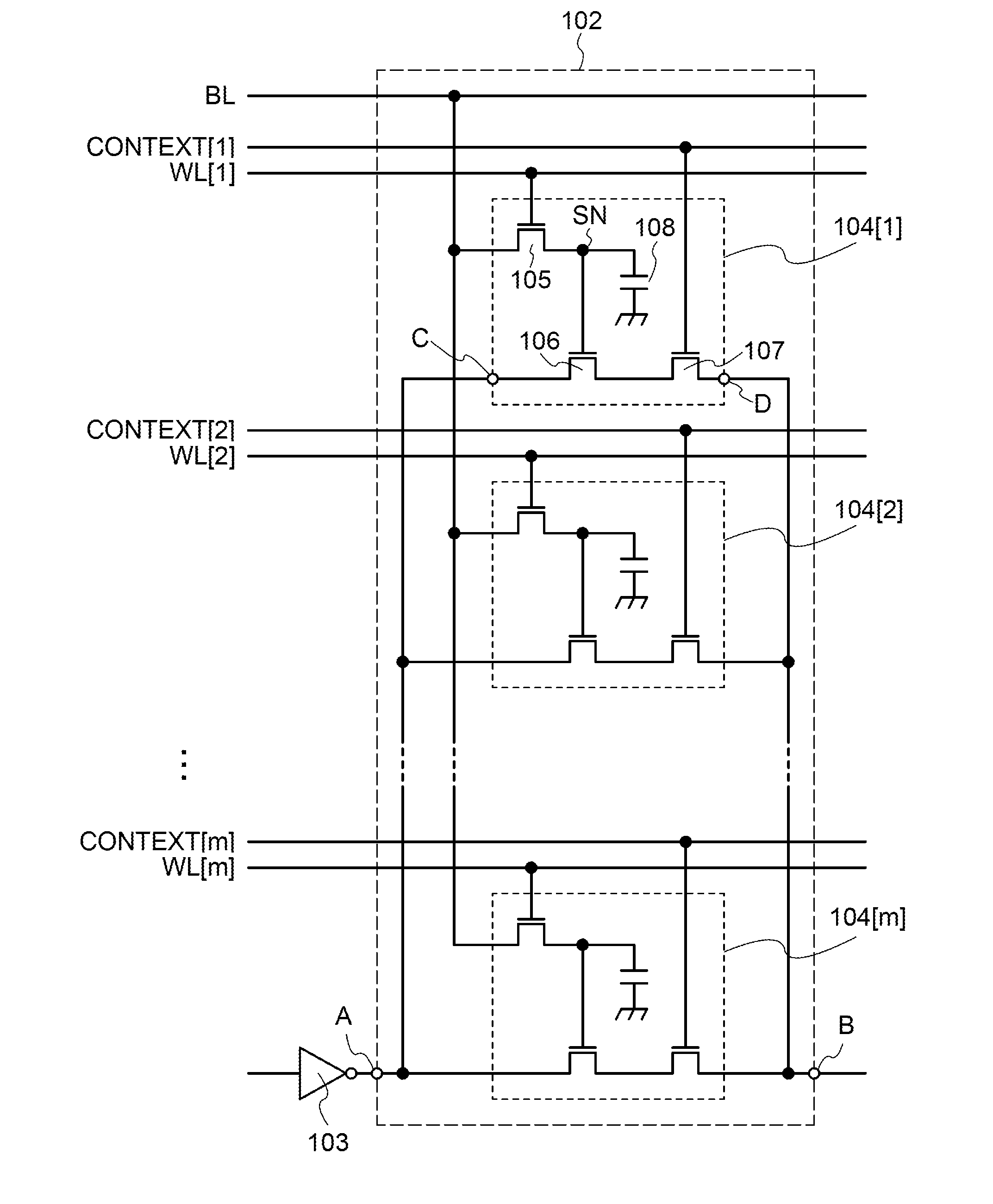
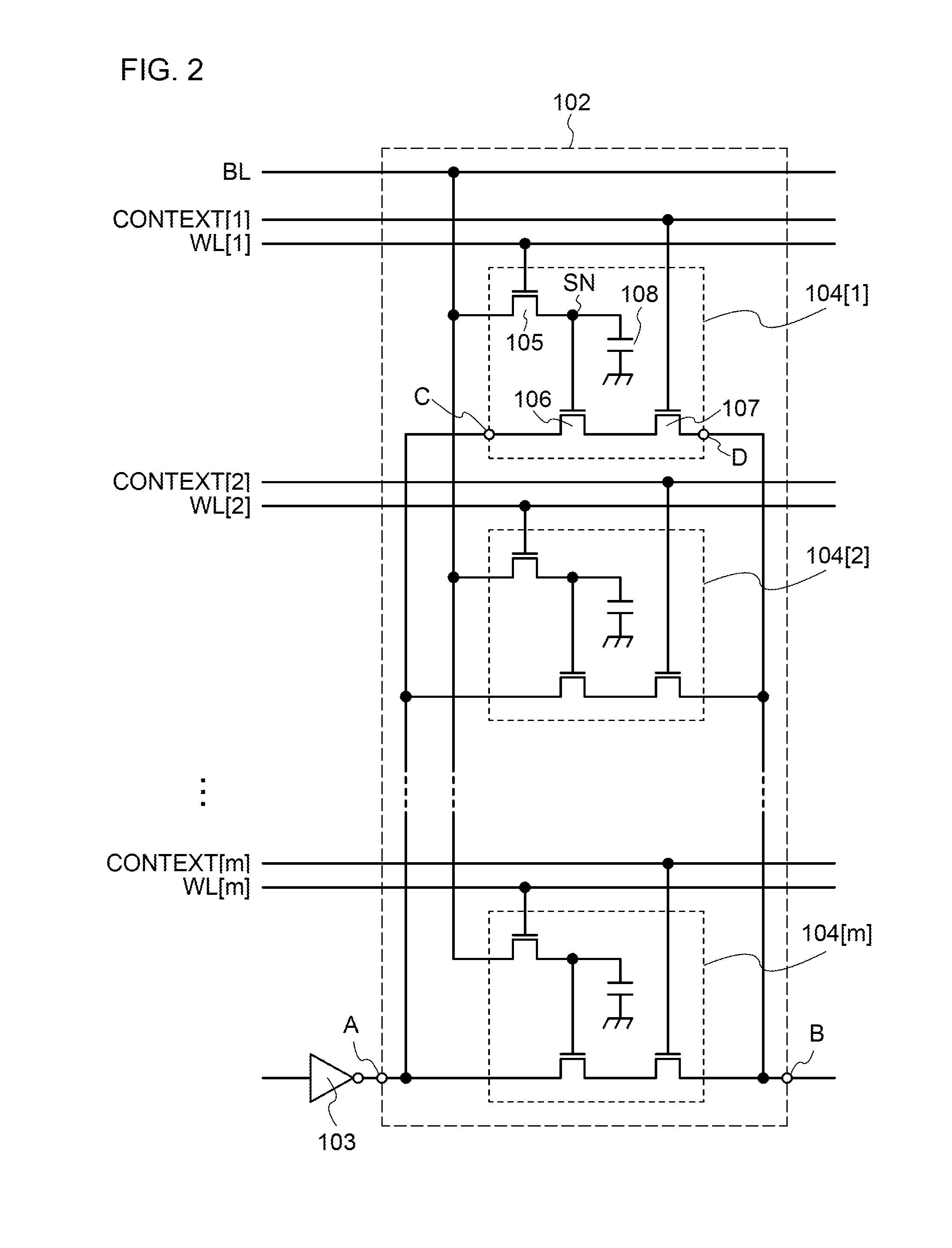
[0057]In this embodiment, a device according to one embodiment of the present invention will be described. In the case where a semiconductor element such as a transistor is used in the device according to one embodiment of the present invention, the device according to one embodiment of the present invention may be referred to as a semiconductor device.

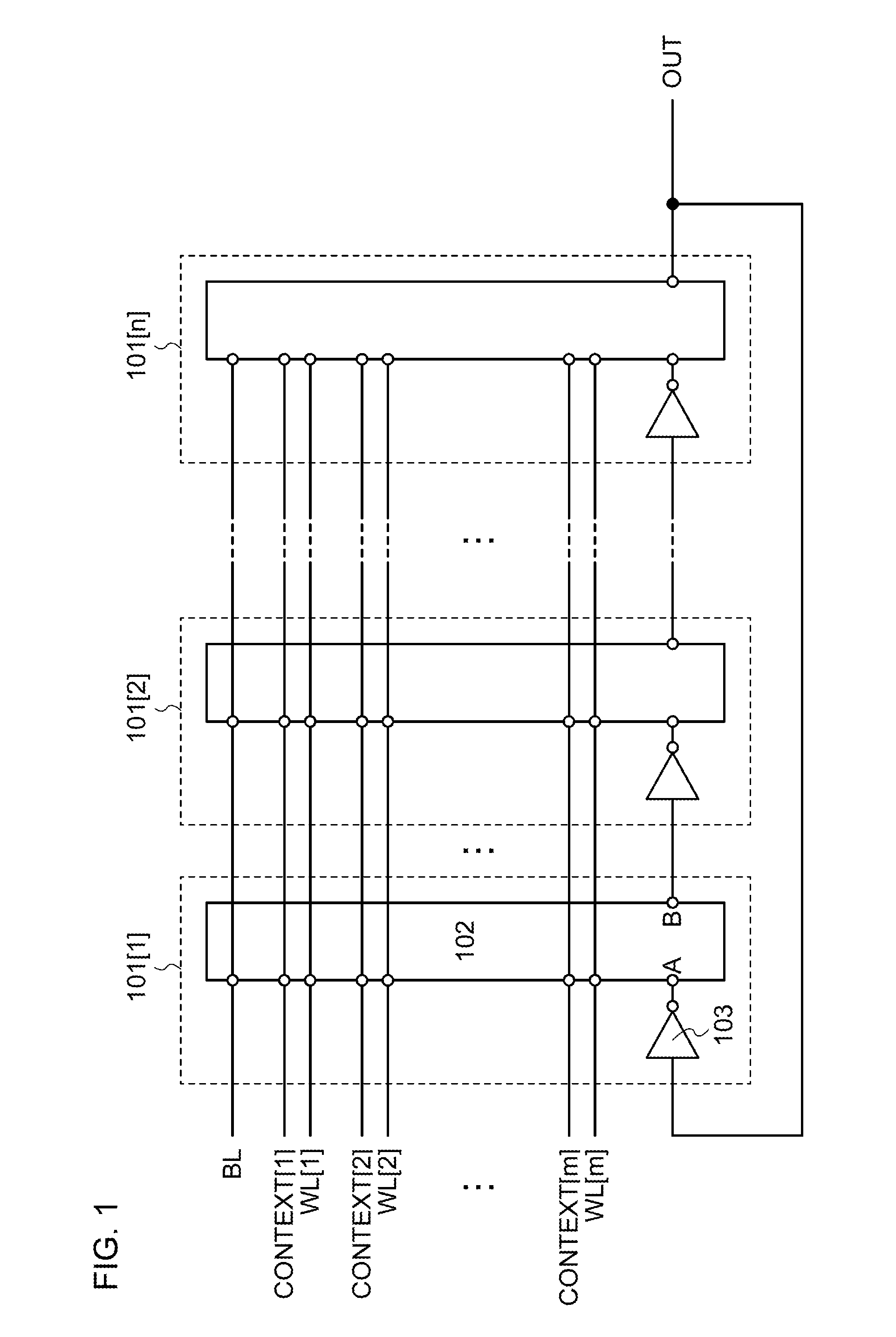
[0058]FIG. 1 illustrates an example of a configuration of a device according to one embodiment of the present invention. The device illustrated in FIG. 1 has a function of generating an alternating-current signal such as a clock signal by oscillating, and may be referred to as an oscillator (or an oscillator circuit). Specifically, the device in FIG. 1 has a function of changing the frequency (or oscillation frequency) of a signal in accordance with input voltage, and may be referred to as a voltage-controlled oscillator (or a voltage-controlled oscillator circuit).

[0059]The device in FIG. 1 includes circuits 101[1] to 101[n] (n is an...

embodiment 2

[0135]In this embodiment, a PLL in which the device described in Embodiment 1 is used will be described.

[0136]A PLL illustrated in FIG. 7 includes a phase comparator 201, a loop filter 202, a voltage-controlled oscillator 203, and a frequency divider 204.

[0137]The phase comparator 201 has a function of detecting a phase difference between two input signals and outputting a detection result as a voltage signal. That is, the phase comparator 201 has a function of outputting a phase difference between a signal with frequency fin and a signal with frequency fout / N as a voltage signal.

[0138]The loop filter 202 has a function of generating a direct-current voltage signal DATA which is to be input to the voltage-controlled oscillator 203. In addition, the loop filter 202 has a function of removing a high-frequency component from an output signal of the phase comparator 201. An example of the loop filter 202 is a low-pass filter.

[0139]The voltage-controlled oscillator 203 has a function of ...

embodiment 3

Example of Cross-Sectional Structure of Semiconductor Device

[0143]FIG. 8 illustrates an example of a cross-sectional structure of the device illustrated in FIG. 1. A transistor 22 corresponds to the transistor 105, and a transistor 23 corresponds to the transistor 106. A region along dashed line A1-A2 shows a structure of the transistors 22 and 23 in the channel length direction, and a region along dashed line A3-A4 shows a structure of the transistors 22 and 23 in the channel width direction. Note that in one embodiment of the present invention, the channel length direction of the transistor 22 is not necessarily aligned with the channel length direction of the transistor 23.

[0144]The channel length direction refers to a direction in which a carrier moves between a source (source region or source electrode) and a drain (drain region or drain electrode), and the channel width direction refers to a direction perpendicular to the channel length direction in a plane parallel to a subst...


PUM


Abstract

A novel PLL is provided. An oscillator circuit includes first to n-th inverters, and first and second circuits. A first terminal of each of the first and second circuits is electrically connected to an output terminal of the i-th inverter. A second terminal of each of the first and second circuits is electrically connected to an input terminal of the (i+1)-th inverter. The first circuit has functions of storing first data, switching between electrically disconnecting the first terminal and the second terminal from each other and setting a resistance between the first terminal and the second terminal to a value based on the first data. The second circuit has functions of storing second data, switching between electrically disconnecting the first terminal and the second terminal from each other and setting a resistance between the first terminal and the second terminal to a value based on the second data.

Description

TECHNICAL FIELD[0001]One embodiment of the present invention relates to a device such as a semiconductor device or a method for driving the device.[0002]Note that one embodiment of the present invention is not limited to the above technical field. The technical field of one embodiment of the invention disclosed in this specification and the like relates to an object, a method, or a manufacturing method. In addition, one embodiment of the present invention relates to a process, a machine, manufacture, or a composition of matter. Specifically, examples of the technical field of one embodiment of the present invention disclosed in this specification include a semiconductor device, a display device, a liquid crystal display device, a light-emitting device, a lighting device, a power storage device, a memory device, a method for driving any of them, and a method for manufacturing any of them.BACKGROUND ART[0003]Phase-locked loops (PLLs) have been actively developed (see Non-Patent Docume...

Claims


Application Information

Patent Timeline
IPC IPC(8): H03K3/356H03K3/012H01L29/786H03K17/0412H03K17/687
CPCH03K3/356086H03K17/04123H03K3/012H01L29/78693H03K17/687H01L29/7869H03K3/0315H03K5/131H03K5/26H03L7/099H03L7/0995H01L27/1225H01L27/1255H03L7/093
Inventor OKAMOTO, YUKIKUROKAWA, YOSHIYUKI
Owner SEMICON ENERGY LAB CO LTD
Why Eureka
Try Eureka