Method, apparatus and system for configuring a protocol stack of an integrated circuit chip

a protocol stack and integrated circuit technology, applied in the field of integrated circuit architectures, can solve the problems of inconvenient use of conventional protocol stacks, large power consumption and chip area, and high bandwidth interconnection between chips using conventional protocol stacks

Active Publication Date: 2015-09-24
SK HYNIX NAND PROD SOLUTIONS CORP
View PDF16 Cites 11 Cited by
  • Summary
  • Abstract
  • Description
  • Claims
  • Application Information

AI Technical Summary

Problems solved by technology

High bandwidth interconnections between chips using conventional protocol stacks require significant power and chip area.
Thus, in app...

Method used


Image

  • Method, apparatus and system for configuring a protocol stack of an integrated circuit chip
  • Method, apparatus and system for configuring a protocol stack of an integrated circuit chip
  • Method, apparatus and system for configuring a protocol stack of an integrated circuit chip

Examples


Embodiment Construction

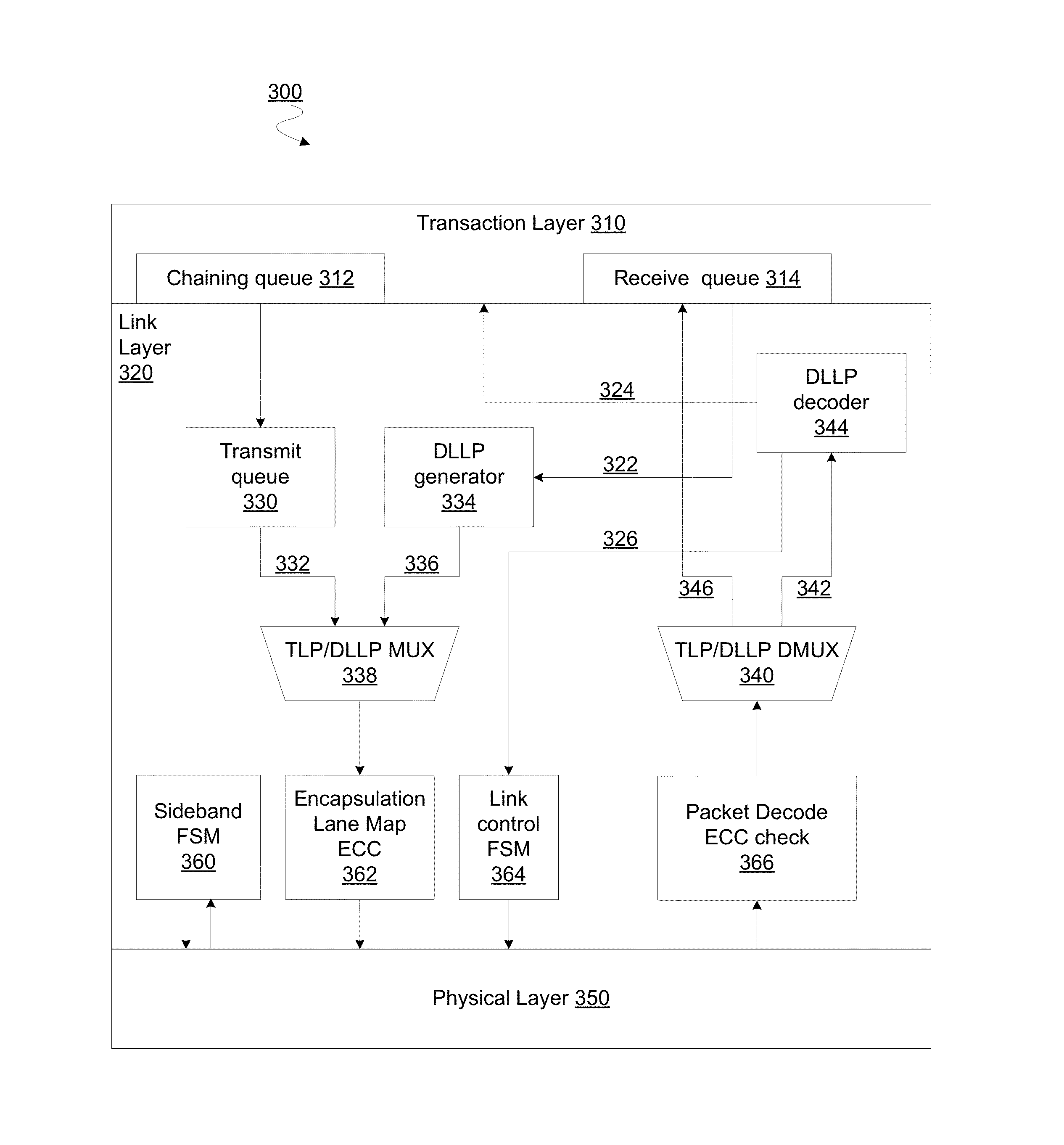
[0018]Embodiments discussed herein variously relate to a protocol stack—for brevity, referred to herein as On-Package Interface (OPI)—including circuitry to provides for efficient communication between different integrated circuit (IC) chips of a packaged device.

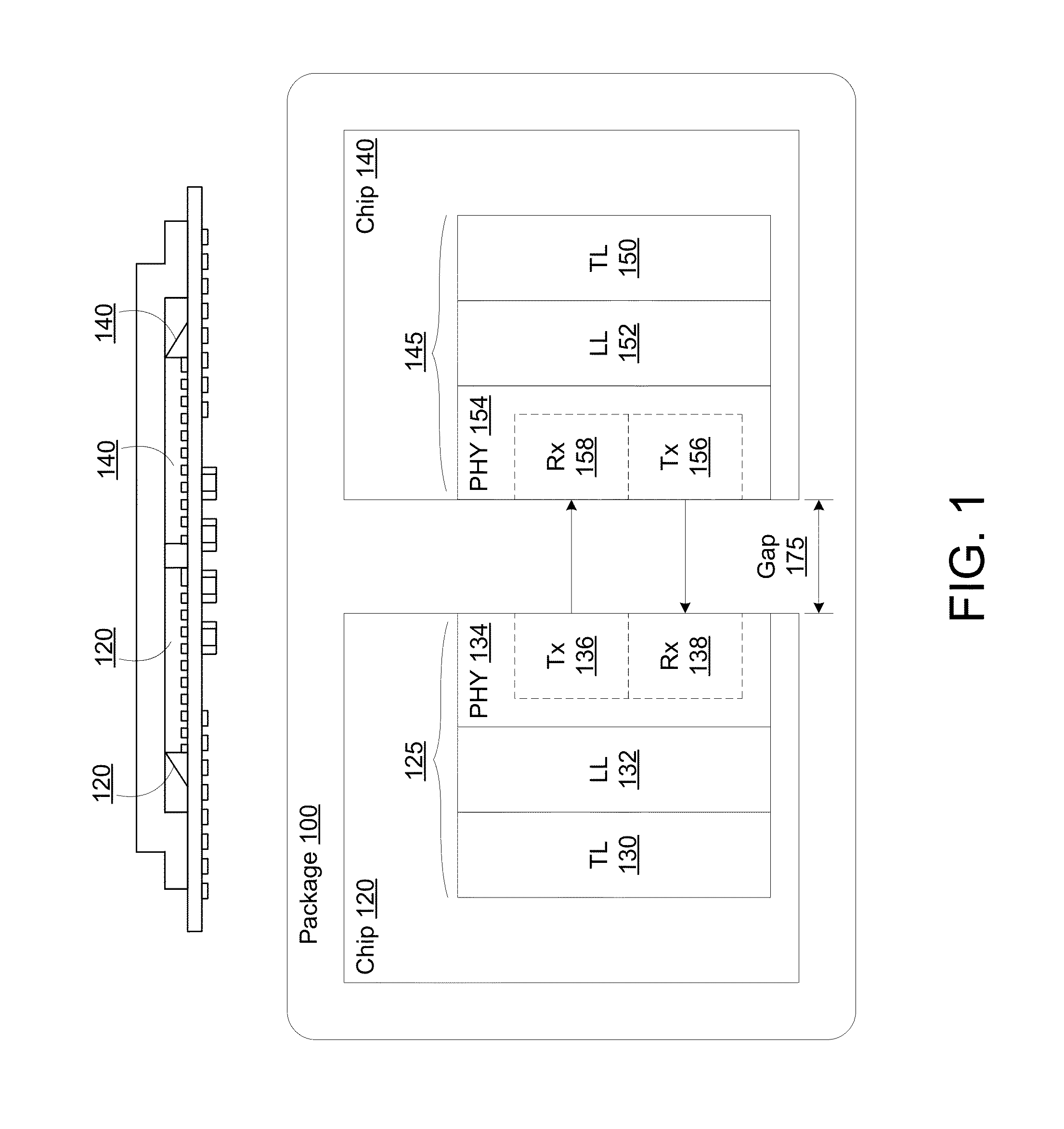
[0019]FIG. 1 is a block diagram of one embodiment of a multichip package (MCP) including at least two chips each comprising a respective on-package interconnect (OPI) protocol stack. The example of FIG. 1 illustrates two chips with stacks; however, any number of chips within a package can be interconnected using the techniques described herein.

[0020]Package 100 may be any type of package that may contain multiple integrated circuit chips. In the example of FIG. 1, package 100 contains chip 120 and chip 140. One or each of such chips may variously include, for example, one or more of a processor, controller, memory chip, graphics processors, etc. In one embodiment, chip 120 includes circuitry comprising a protocol stack 125 i...


PUM


Abstract

Techniques and mechanisms for configuring an integrated circuit (IC) chip to implement a protocol stack. In an embodiment, a transaction layer of the IC chip is operable to exchange with a link layer of the IC chip transaction layer packets (TLPs) having a format compatible with one defined in a Peripheral Component Interconnect Express™ (PCIe™) specification. Configuration circuitry of the IC chip provides for configuration of a first protocol stack including the transaction layer, circuitry of the link layer and a first physical layer of the IC chip. The configuration circuitry further provides for an alternative configuration of a second protocol stack including the transaction layer, circuitry of the link layer and a second physical layer of the IC chip. In another embodiment, the first protocol stack supports single-ended signaling to communicate TLP information, whereas the second protocol stack supports differential signaling to communicate TLP information.

Description

CLAIM OF PRIORITY[0001]This application claims the benefit of priority of Malaysia Patent Application No. PI2014700666, filed Mar. 20, 2014, titled “METHOD, APPARATUS AND SYSTEM FOR CONFIGURING A PROTOCOL STACK OF AN INTEGRATED CIRCUIT CHIP”, which is incorporated by reference in its entirety.BACKGROUND[0002]1. Technical Field[0003]Embodiments of the invention relate to integrated circuit architectures. More particularly, embodiments of the invention relate to high-bandwidth on-package protocol stacks.[0004]2. Background Art[0005]High bandwidth interconnections between chips using conventional protocol stacks require significant power and chip area. Thus, in applications requiring significantly reduced power consumption and / or smaller chip area, these conventional protocol stacks are not desirable.BRIEF DESCRIPTION OF THE DRAWINGS[0006]The various embodiments of the present invention are illustrated by way of example, and not by way of limitation, in the figures of the accompanying ...

Claims


Application Information

Patent Timeline
IPC IPC(8): G06F13/42
CPCG06F13/4221G06F13/122G06F13/4265Y02D10/00
Inventor SPRY, BRYAN L.SONG, MARCUS W.RANGARAJ, DEEPAK M.ANANTHAKRISHNAN, AVINASH N.HAYES, ROBERT J.WOOD, AIMEE D.LETENDRE, ADAM E.BOSWELL, BRENT R.
Owner SK HYNIX NAND PROD SOLUTIONS CORP
Why Eureka
Try Eureka