Electronic device with high electrostatic protection

a technology of electrostatic protection and electrostatic shielding, applied in the direction of photometry using electric radiation detectors, optical radiation measurement, instruments, etc., can solve the problems of increasing costs, achieve significant improvement of substrate area utilization, increase discharge distance, and improve electrostatic protection ability

Active Publication Date: 2015-10-01
PIXART IMAGING INC
View PDF22 Cites 5 Cited by
  • Summary
  • Abstract
  • Description
  • Claims
  • Application Information

AI Technical Summary

Benefits of technology

[0021]In the electronic device according to some embodiments of the present disclosure, it is able to increase the discharge distance between electrical pins and the discharge surface by bending the electrical pins backward (an opposite direction of emitting and sensing light) so as to improve the electrostati...

Problems solved by technology

However, using a large lens can increase the manufa...

Method used


Image

  • Electronic device with high electrostatic protection
  • Electronic device with high electrostatic protection
  • Electronic device with high electrostatic protection

Examples


Embodiment Construction

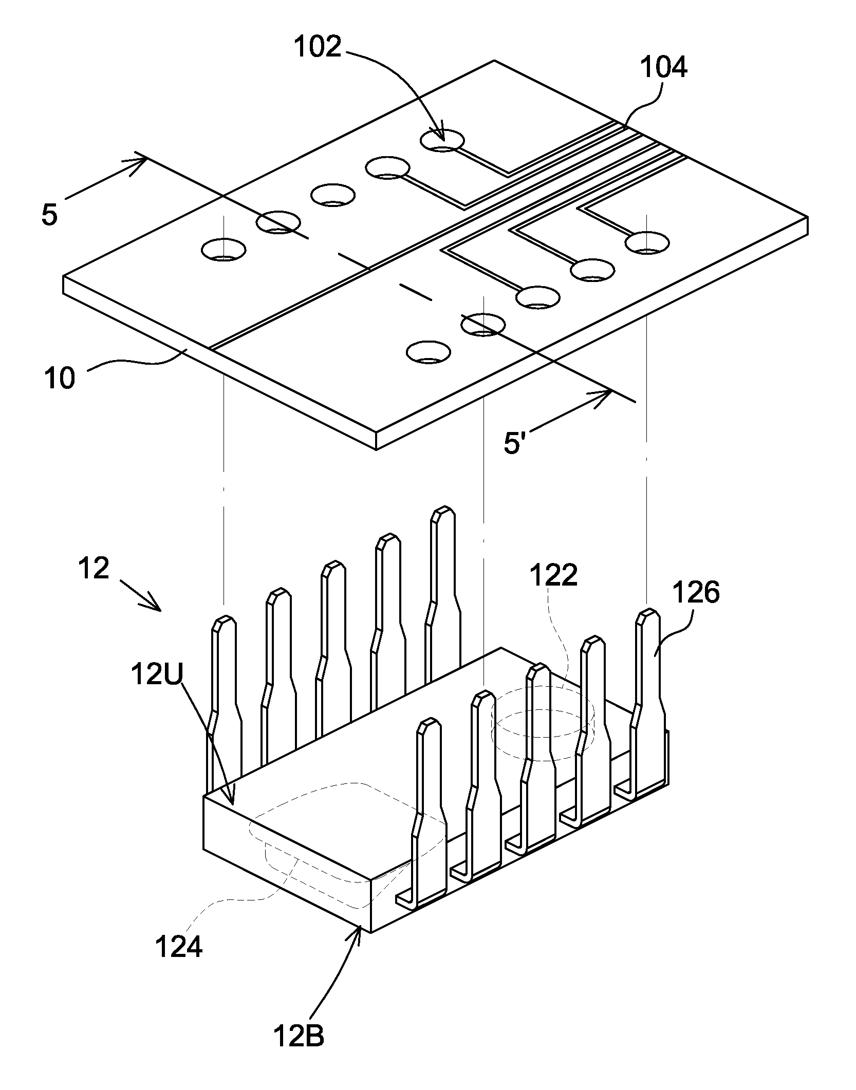
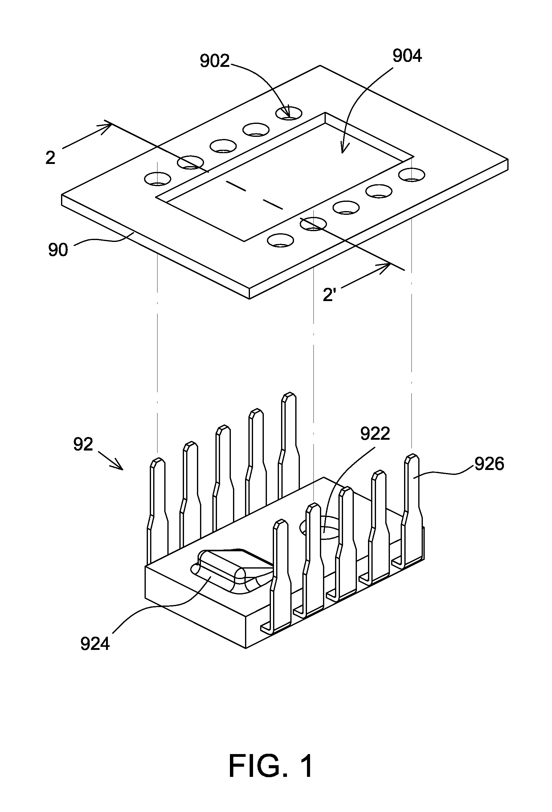
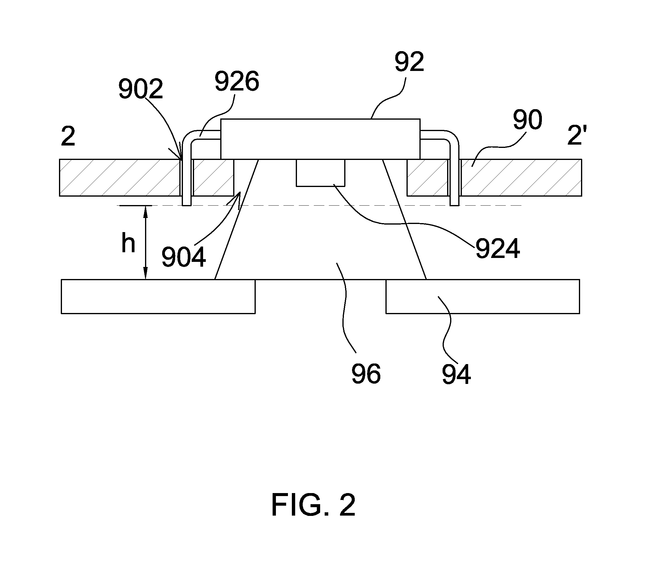
[0029]It should be noted that, wherever possible, the same reference numbers will be used throughout the drawings to refer to the same or like parts.

[0030]Referring to FIG. 3, it is a schematic diagram of the electronic device 1 according to one embodiment of the present disclosure. It should be mentioned that although an optical mouse is shown herein, it is not to limit the present disclosure and the electronic device 1 may be, for example, a portable electronic device such as a cell phone, a tablet computer or an optical navigation device. The electronic device 1 includes a light source configured to illuminate a reflective surface and an image sensor configured to receive reflected light from the reflective surface. For example, when the electronic device 1 is an optical mouse, the reflective surface is, for example, a working surface S (as shown in FIG. 3). When the electronic device 1 is other portable devices such as a proximity sensor, the electronic device 1 is configured to...


PUM


Abstract

An electronic device including a substrate and an optoelectronic device package is provided. The optoelectronic device package includes a light source, an image sensor and a plurality of connecting pins. The light source is configured to emit light toward a direction of a bottom surface of the optoelectronic device package. The image sensor is configured to receive reflected light from the direction of the bottom surface. The connecting pins are bended toward an opposite direction of the direction of the bottom surface and electrically connected to the substrate thereby increasing a discharge path of the electrostatic discharge.

Description

RELATED APPLICATIONS[0001]The present application is based on and claims priority to Taiwanese Application Number 103112243, filed Apr. 1, 2014, the disclosure of which is hereby incorporated by reference herein in its entirety.BACKGROUND[0002]1. Field of the Disclosure[0003]This disclosure generally relates to an electronic device and, more particularly, to an electronic device capable of improving the electrostatic protection ability of the optoelectronic device and the utilization of the substrate area.[0004]2. Description of the Related Art[0005]The optical mouse generally includes an image sensor package which has the function of emitting light and sensing light. For example, FIG. 1 is a schematic diagram of an image sensor package 92 and a circuit board 90 included in a conventional optical mouse. The image sensor package 92 includes a light emitting diode 922, an image sensor 924 and a plurality of connecting pins 926. The circuit board 90 includes a plurality of metallized h...

Claims


Application Information

Patent Timeline
IPC IPC(8): G01J1/02
CPCG01J1/0252G01J1/0271G01J1/0233G01J1/4228G01J2001/0276G06F3/0317
Inventor WANG, TSUNG-FACHANG, YEN-MINCHUNG, CHING-LIN
Owner PIXART IMAGING INC
Why Eureka
Try Eureka