Pixel structure

a pixel and structure technology, applied in non-linear optics, instruments, optics, etc., can solve the problems of large loss of aperture ratio of pixel, more severe color shifting, etc., and achieve the effect of improving the color shifting issue of a large-sized panel and reducing the aperture ratio

Active Publication Date: 2015-10-08
TCL CHINA STAR OPTOELECTRONICS TECH CO LTD
View PDF5 Cites 9 Cited by
  • Summary
  • Abstract
  • Description
  • Claims
  • Application Information

AI Technical Summary

Benefits of technology

[0008]An object of the present invention is to provide a pixel structure that improves the color shifting issue of a large-sized panel without reducing aperture ratio by applying voltages that supply different potentials to a first and a second sub common electrodes of a color filter substrate in order to make a first voltage difference between a first sub pixel electrode and a first sub common electrode greater than or less than a second voltage difference between a second sub pixel electrode and a second sub common electrode.
[0028]The efficacy of the present invention is that the present invention provides a pixel structure, in which voltages of different potentials are respectively applied to first and second sub common electrodes of a color filter substrate so as to make a first voltage difference between a first sub pixel electrode and the first sub common electrode greater than or less than a second voltage difference between a second sub pixel electrode and the second sub common electrode, whereby the need for an additional gate line and formation of a charge sharing capacitor on the pixel electrode side that are found in the prior art can be avoided and further, it is possible to reduce one or two thin-film transistors to avoid loss of aperture ratio so as to improve the color shift problem of large view angles of a large-sized panel without reducing the aperture ratio.

Problems solved by technology

The larger the view angle is, the more severe the color shifting will be.
A pixel structure having such an arrangement can achieve suppressing of color shifting; however, three thin-film transistors and two gate lines are needed for each pixel to control the charging of the pixel and this causes a great loss of aperture ratio of the pixel.

Method used


Image

  • Pixel structure
  • Pixel structure
  • Pixel structure

Examples


Embodiment Construction

[0041]To further expound the technical solution adopted in the present invention and the advantages thereof, a detailed description is given to preferred embodiments of the present invention and the attached drawings.

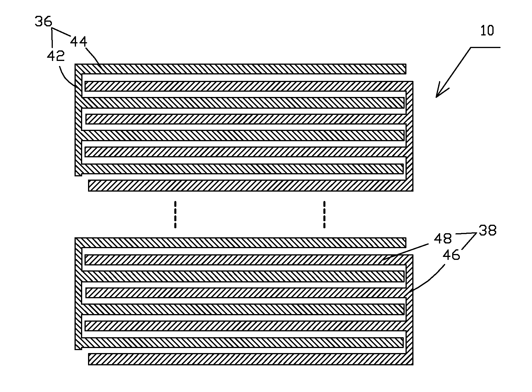
[0042]Referring to FIGS. 3-8, the present invention provides a pixel structure 10, which comprises: a TFT (Thin-Film Transistor) substrate 20, a CF (Color Filter) substrate 30 opposite to the TFT substrate 20, and a liquid crystal layer 40 arranged between the TFT substrate 20 and the CF substrate 30.

[0043]The TFT substrate 20 comprises a first transparent substrate 22 and a pixel electrode 24 formed on a surface of the first transparent substrate 22 that faces the CF substrate 30. The CF substrate 30 comprises a second transparent substrate 32 and a common electrode 34 formed on a surface of the second transparent substrate 32 that faces the TFT substrate 20. The pixel electrode 24 comprises a first sub pixel electrode 26 and a second sub pixel electrode 28. The common...


PUM

PropertyMeasurementUnit
transparentaaaaaaaaaa
driving voltagesaaaaaaaaaa
voltageaaaaaaaaaa

Abstract

The present invention provides a pixel structure, which includes a TFT substrate (20), a CF substrate (30) and a liquid crystal layer (40). The TFT substrate (20) includes a first transparent substrate (22) and a pixel electrode (24). The CF substrate (30) includes a second transparent substrate (32) and a common electrode (34). The pixel electrode (24) includes a first sub pixel electrode (26) and a second sub pixel electrode (28). The common electrode (34) includes a first sub common electrode (36) and a second sub common electrode (38). The first sub pixel electrode (26) and the first sub common electrode (36) have a first voltage difference and the second sub pixel electrode (28) and the second sub common electrode (38) have a second voltage difference. The first voltage difference is greater than or less than the second voltage difference.

Description

BACKGROUND OF THE INVENTION[0001]1. Field of the Invention[0002]The present invention relates to the field of liquid crystal display technology, and in particular to a pixel structure.[0003]2. The Related Arts[0004]Liquid crystal displays have a variety of advantages, such as thin device body, low power consumption, and being free of radiation, and are thus widely used. Most of the liquid crystal displays that are currently available in the market are backlighting liquid crystal displays, which comprise a liquid crystal display panel and a backlight module. The operation principle of the liquid crystal display panel is that, with liquid crystal molecules interposed between two parallel glass substrates, a driving voltage is applied to the two glass substrates to control the rotation direction of the liquid crystal molecules in order to refract out light emitting from the backlight module to generate an image. Since the liquid crystal display panel does not emit light by itself, ligh...

Claims


Application Information

Patent Timeline
Patent Type & Authority Applications(United States)
IPC IPC(8): G02F1/1343G02F1/1362G02F1/1335G02F1/1368
CPCG02F1/134309G02F1/1368G02F2001/134318G02F1/133514G02F2001/134345G02F1/136213G02F1/134345G02F1/1343G02F1/1362G02F1/134318
Inventor LO, SHIHHSUNGUO, JINBOHUANG, SHISHUAI
Owner TCL CHINA STAR OPTOELECTRONICS TECH CO LTD
Why Eureka
Try Eureka