Conductive film, display device equipped with same and method for determining pattern of conductive film

a display device and conductive film technology, applied in the field of conductive film, can solve the problems of insufficient improvement of the moire recognition property, promoting the visual recognition of moire due to intensity, and varying the spatial frequency characteristics of the wiring pattern of the mesh-like conductive wiring. achieve the effect of preventing the occurrence, improving visibility, and reducing the number of occurrences

Active Publication Date: 2015-10-08
FUJIFILM CORP
View PDF20 Cites 32 Cited by
  • Summary
  • Abstract
  • Description
  • Claims
  • Application Information

AI Technical Summary

Benefits of technology

[0020]An object of the present invention is to solve the problems of the aforementioned conventional techniques and to provide a conductive film, which can inhibit the occurrence of moire and can greatly improve recognition property, a display device equipped with the conductive film, and a method for determining a pattern of a conductive film.
[0021]Particularly, in a case in which a conductive film installed on a display unit of a display device has a plurality of disconnection portions in mesh-like wiring having a mesh pattern composed of thin metal wires, moire occurs. Accordingly, another object of the present invention is to provide a conductive film, which can inhibit the occurrence of moire and greatly improve the recognition property even in such a case, a display device equipped with the conductive film, and a method for determining a pattern of a conductive film.
[0022]Furthermore, particularly, in a case in which a transparent conductive film having mesh-like wiring including a plurality of disconnection portions is used as an electrode for a touch panel that needs to be made into a large-sized touch panel and to have higher resolution, when the conductive film is superimposed on a black matrix of a display unit of the display device and visually recognized, moire occurs, and thus greatly impairs image quality. Accordingly, the other object of the present invention is to provide a conductive film, which can inhibit the occurrence of moire and can greatly improve the visibility of display on the touch panel even in such a case, a display device equipped with the conductive film, and a method for determining a pattern of a conductive film.
[0040]Being constituted as above according to the present invention, it is possible to inhibit the occurrence of moire and to greatly improve visibility, even in a case in which a conductive film installed on a display unit of a display device has a plurality of disconnection portions in mesh-like wiring having a mesh pattern composed of thin metal wires.
[0041]Particularly, even in a case in which a transparent conductive film having mesh-like wiring including a plurality of disconnection portions is used as an electrode for a touch panel that needs to be made into a large-sized touch panel and to have higher resolution, according to the present invention, it is possible to inhibit the occurrence of moire that greatly impairs image quality and to greatly improve the visibility of display on the touch panel, when the conductive film is superimposed on a black matrix of a display unit of the display device and visually recognized.

Problems solved by technology

Since human perception of moire is affected by intensity as well as frequency, even at a frequency at which moire is not visually recognized in the technique of JP 2009-117683 A, moire may be visually recognized depending on the intensity, and thus there is a problem in that the moire recognition property is not improved satisfactorily.
Particularly, when the technique disclosed in JP 2009-117683 A is applied to a conductive film for a touch panel, it is necessary to provide a plurality of cut portions (breaks) in the mesh-like conductive wiring, and if the cut portions are provided, there is a problem in that the spatial frequency characteristics of the wiring pattern of the mesh-like conductive wiring vary.
In addition, since the conductive film is pressed with a human finger, a minute distortion occurs between the BM / wiring patterns, and thus there is a problem in that visual recognition of moire due to intensity is promoted.
Accordingly, when the technique disclosed in JP 2009-117683 A is applied to a conductive film for a touch panel, there is a problem in that the improvement in moire recognition property is not satisfactory.
However, in the conventional technique, such a point has not been discussed.
Consequently, the regular period of the disconnections exerts an influence on the visually recognized moire, and this leads to a problem in that the moire recognition property cannot be sufficiently improved.

Method used


Image

  • Conductive film, display device equipped with same and method for determining pattern of conductive film
  • Conductive film, display device equipped with same and method for determining pattern of conductive film
  • Conductive film, display device equipped with same and method for determining pattern of conductive film

Examples


examples

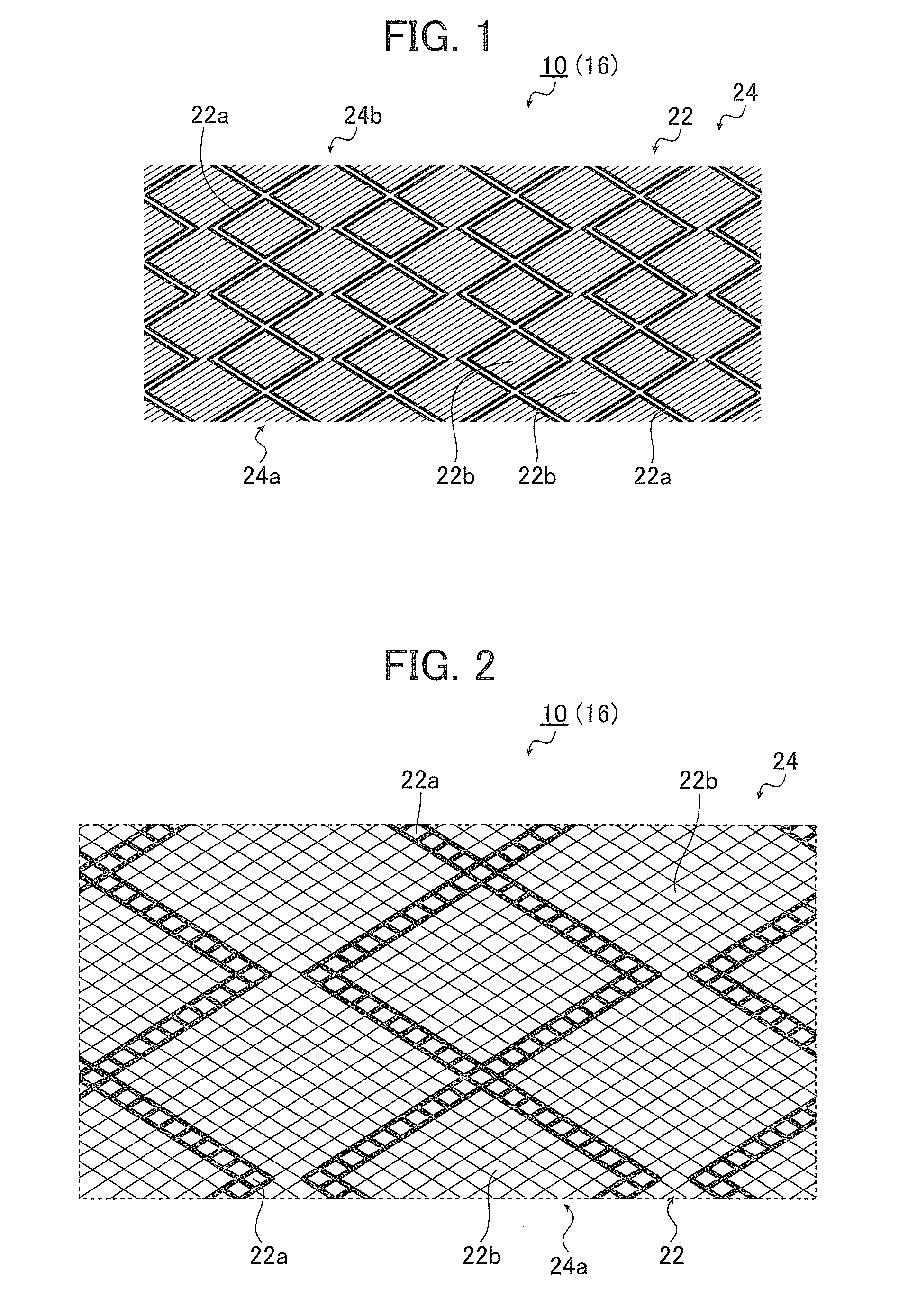
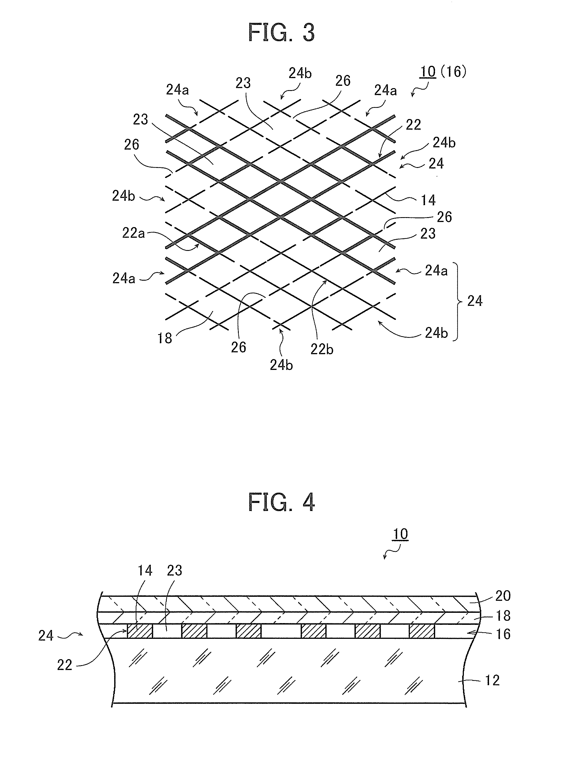
[0158]A mesh pattern 70 shown in FIG. 16 was prepared as a simulation sample of Comparative example 1. The mesh pattern 70 of Comparative example 1 was a wiring pattern constituted with an electrode wiring pattern 74 of an X electrode 72 constituting an effective electrode region and a dummy electrode wiring pattern 78 of 4 dummy electrodes 76a, 76b, 76c, and 76d. The mesh pattern 70 had a plurality of disconnection portions 84 each of which was regularly provided at the center of each of 4 sides composed of thin metal wires 82 that formed a mesh shape of rhomboids of all of openings 80 formed by the dummy electrode wiring pattern 78. In the side between the electrode wiring pattern 74 and the dummy electrode wiring pattern 78, the disconnection portion 84 was also provided in a central position of each of the thin metal wires 82 between the patterns. In the example shown in FIG. 16, for simplifying the drawing, the disconnection portion 84 is shown only in the dummy electrode wirin...


PUM


Abstract

The conductive film which can inhibit the occurrence of moire and can greatly improve recognition property, a display device equipped with the conductive film, and a method for determining a pattern of a conductive film are provide. In the conductive film, a spectral intensity of moire of a lowest frequency is equal to or less than −3.6 expressed in terms of common logarithm, and the spectral intensity is represented by convolution of spatial frequency characteristics of the mesh pattern that are obtained at least when the mesh pattern is observed from a front side and spatial frequency characteristics of the pixel array pattern of the display unit that are obtained at least when the pixel array pattern is observed from a front side. The mesh pattern may include a plurality of disconnection portions.

Description

CROSS-REFERENCE TO RELATED APPLICATIONS[0001]This application is a Continuation of PCT International Application No. PCT / JP2013 / 083001 filed on Dec. 9, 2013, which claims priority under 35 U.S.C. §119(a) to Japanese Patent Application No. 2012-276175 filed on Dec. 18, 2012. Each of the above application(s) is hereby expressly incorporated by reference, in its entirety, into the present application.BACKGROUND OF THE INVENTION[0002]The present invention relates to a conductive film, a display device equipped with the conductive film, and a method for determining a pattern of a conductive film. Specifically, the present invention relates to a conductive film, which is used as a mesh transparent conductive film, and has a mesh pattern designed in consideration of an electrode such that a spectral intensity and a frequency of visually recognized moire are respectively within predetermined ranges of intensity and frequency, a display device equipped with the conductive film, and a method ...

Claims


Application Information

Patent Timeline
Patent Type & Authority Applications(United States)
IPC IPC(8): G06F3/047G06F3/044
CPCG06F3/047G06F2203/04112G06F2203/04103G06F3/044G06F3/041H05K9/0096G06F3/0412G06F3/0445G06F3/0446
Inventor IWAMI, KAZUCHIKANAKAMURA, HIROSHIGE
Owner FUJIFILM CORP
Why Eureka
Try Eureka