Solid-state imaging apparatus

a solid-state imaging and apparatus technology, applied in the field of solid-state imaging apparatus, can solve the problems of deteriorating noise suppression effect, difficult to obtain sufficient gain in fine pixel, etc., and achieve the effect of reducing ktc nois

Active Publication Date: 2015-10-08
PANASONIC INTELLECTUAL PROPERTY MANAGEMENT CO LTD
View PDF2 Cites 23 Cited by
  • Summary
  • Abstract
  • Description
  • Claims
  • Application Information

AI Technical Summary

Benefits of technology

[0011]The solid-state imaging apparatus according to the present invention can significantly reduce kTC noise by using a negative feedback amplifying circuit.

Problems solved by technology

As a result, it becomes difficult to obtain a sufficient gain in a fine pixel, which deteriorates a noise suppression effect.

Method used


Image

  • Solid-state imaging apparatus
  • Solid-state imaging apparatus
  • Solid-state imaging apparatus

Examples


first exemplary embodiment

[0028]An overall configuration of a solid-state imaging apparatus according to a first exemplary embodiment will be described.

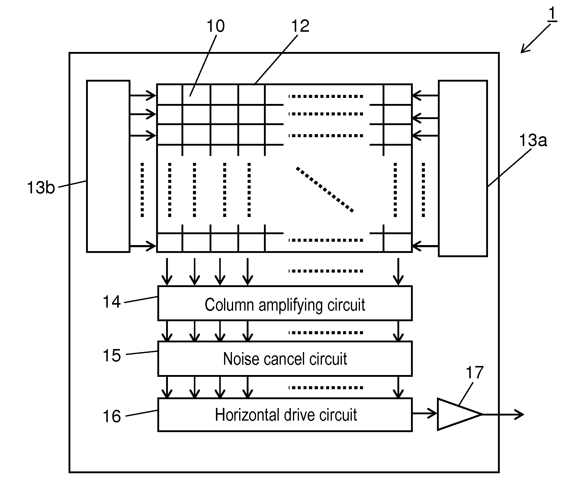
[0029]FIG. 1 is a block diagram illustrating an overall configuration of the solid-state imaging apparatus according to the first exemplary embodiment. Solid-state imaging apparatus 1 illustrated in FIG. 1 includes pixel unit 12 having a plurality of pixels 10 arranged in a matrix on a semiconductor substrate, row signal drive circuits 13a and 13b, column amplifying circuit 14 arranged for each column, noise cancel circuit 15, such as a correlated double sampling (CDS) circuit, arranged for each column, horizontal drive circuit 16, and output stage amplifier 17.

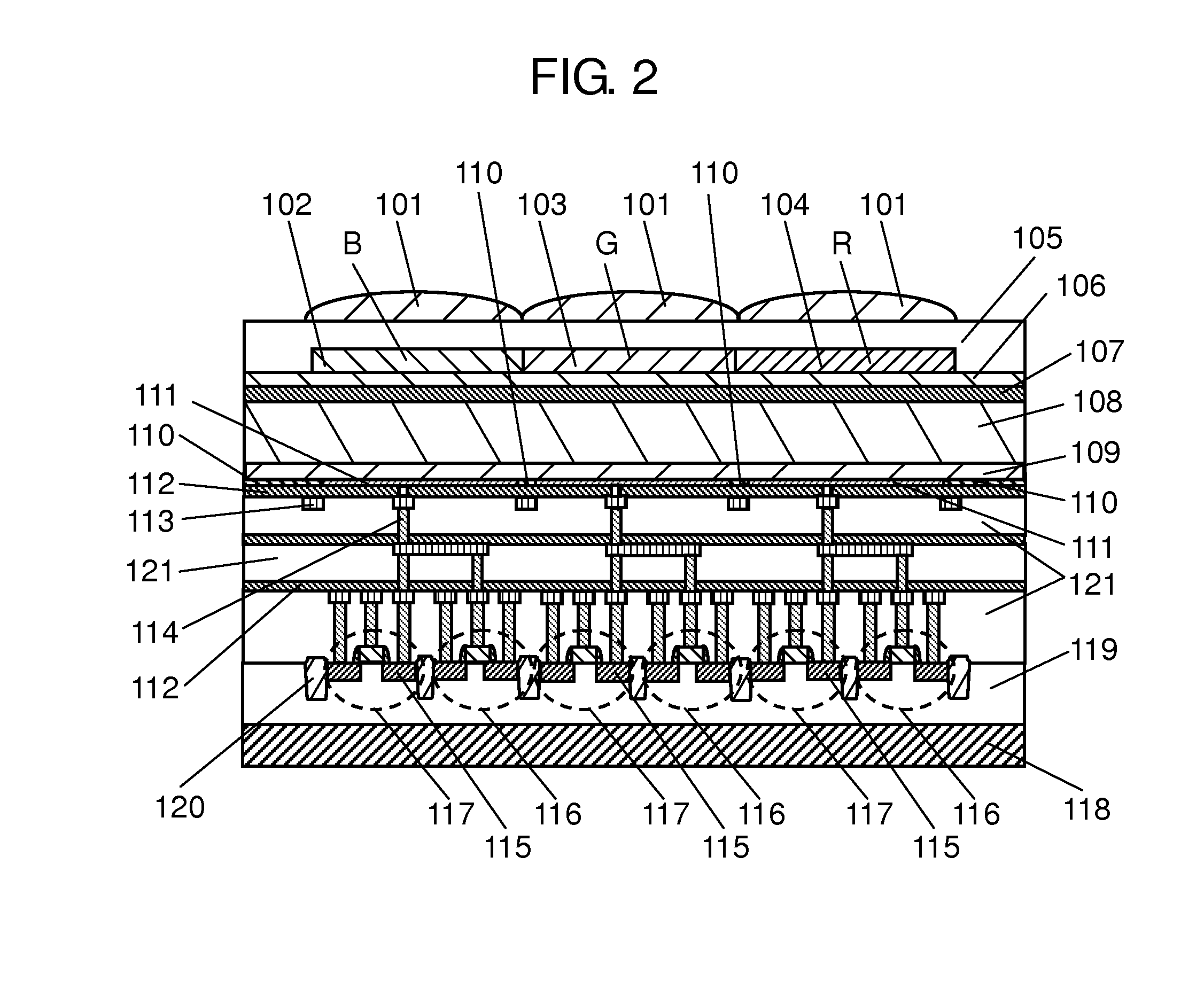
[0030]FIG. 2 is a sectional view illustrating the structure of the solid-state imaging apparatus according to the first exemplary embodiment for three pixels. In an actual solid-state imaging apparatus, ten million pixels, for example, are arranged in the pixel unit 12 in a matrix. As illustrated in FI...

second exemplary embodiment

[0067]FIG. 5 is a diagram illustrating one example of a circuit of pixel 10 belonging to an mth row (m is a natural number) and an nth column (n is a natural number) of pixel unit 12, and its control circuit according to a second exemplary embodiment.

[0068]The different point from the circuit structure according to the first exemplary embodiment is such that amplifying transistor 116 is connected to cutoff transistor 302 via selection transistor 501. Specifically, one of a source and a drain of selection transistor 501 is connected to the other one of the source and the drain of amplifying transistor 116. The other one of the source and the drain of selection transistor 501 is connected to one of the source and the drain of cutoff transistor 302. The other one of the source and the drain of selection transistor 501 is connected to other one 303 of the source and the drain of reset transistor 117.

[0069]FIG. 6 is a timing chart illustrating a driving method for pixels on the mth row i...

third exemplary embodiment

[0084]Next, a third exemplary embodiment will be described.

[0085]FIG. 7 is a diagram illustrating one example of a circuit of pixel 10 belonging to an mth row (m is a natural number) and an nth column (n is a natural number) of pixel unit 12, and its control circuit according to a third exemplary embodiment.

[0086]The pixel unit 12 includes, for each column, a column signal line 702 which is connected to a reference potential or outputs a pixel signal from the pixel 10, and a source line 701 connected to third power supply voltage VDD3. One of the source and the drain of amplifying transistor 116 is connected to column signal line 702. The other one of the source and the drain of cutoff transistor 302 is connected to source line 701. One end of column signal line 702 is connected to a signal output unit (terminal E) or a reference potential (terminal F) via terminal TE3. Source line 701 and column signal line 702 provided for each column are commonly connected to a plurality of pixel...


PUM


Abstract

The present invention provides a solid-state imaging apparatus that can significantly reduce kTC noise by using a negative feedback amplifying circuit. A solid-state imaging apparatus includes a pixel unit including a plurality of pixels arranged on a semiconductor substrate in a matrix, the pixel unit including, for each column, a source line and a column signal line, each of the plurality of pixels including: a photoelectric conversion unit that generates a signal charge corresponding to incident light; a storage unit storing the signal charge; a reset transistor; an amplifying transistor; and a cutoff transistor, wherein the amplifying transistor and the cutoff transistor form a negative feedback amplifying circuit. With this configuration, kTC noise can significantly be reduced.

Description

TECHNICAL FIELD[0001]The present invention relates to a solid-state imaging apparatus, and more particularly to a stacked solid-state imaging apparatus.BACKGROUND ART[0002]PTL 1 describes a stacked solid-state imaging apparatus. The stacked solid-state imaging apparatus described in PTL 1 generates noise when resetting signal charges. Specifically, in the case where a shape of a reset pulse in the off is sharp, to which one of a source and a drain of a reset transistor charges on a channel move is randomly determined. Therefore, this appears as kTC noise. The kTC noise is also generated with capacitance coupling between a reset signal line and a pixel electrode, and the like.[0003]In addition, a stacked solid-state imaging apparatus cannot completely cancel kTC noise even by using correlated double sampling. This is because, in the stacked solid-state imaging apparatus, charges cannot completely be transferred due to a structure in which a photoelectric conversion unit provided abov...

Claims


Application Information

Patent Timeline
Patent Type & Authority Applications(United States)
IPC IPC(8): H04N5/363H04N5/378
CPCH04N5/378H04N5/363H04N25/65H04N25/77H04N25/79H10K39/32H04N25/75H04N25/76H04N25/766
Inventor YAZAWA, KEISUKEISHII, MOTONORIHIROSE, YUTAKAKATO, YOSHIHISAMATSUNAGA, YOSHIYUKI
Owner PANASONIC INTELLECTUAL PROPERTY MANAGEMENT CO LTD
Why Eureka
Try Eureka