

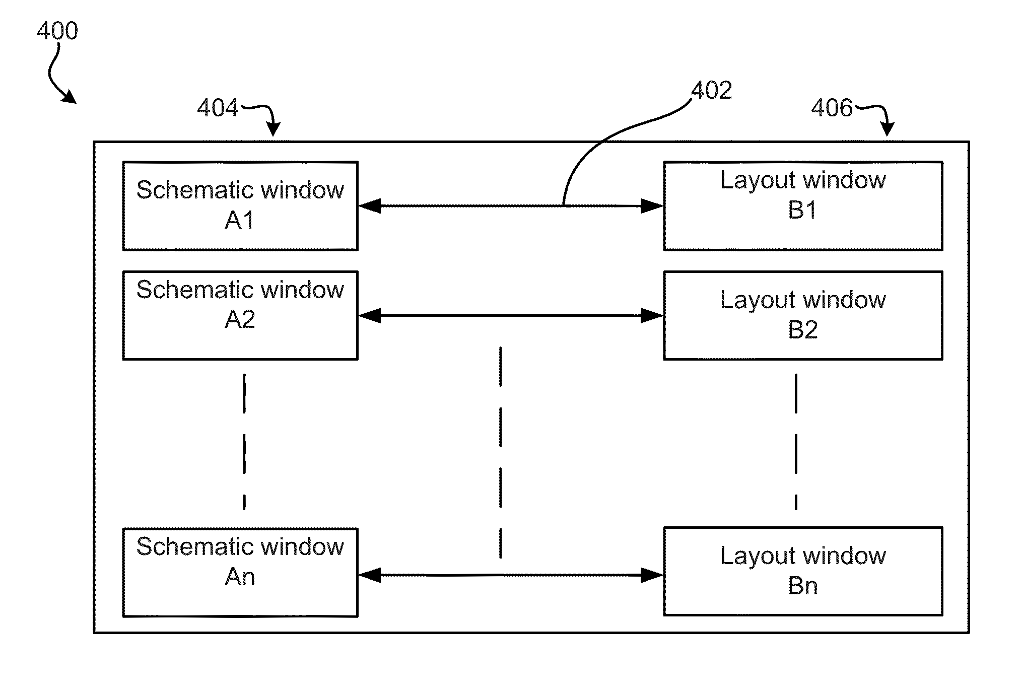
Viewing multi paired schematic and layout windows on printed circuit board (PCB) design software and tools
a printed circuit board and multi-paired technology, applied in the direction of cad circuit design, instrumentation, transportation and packaging, etc., can solve the problems of limiting, and it is not possible for the user/user to zoom in on both the driver and the receiver portions of the layout window
- Summary
- Abstract
- Description
- Claims
- Application Information
AI Technical Summary
Benefits of technology
Problems solved by technology
Method used
Image

Examples
Embodiment Construction
[0014]The following description is made for the purpose of illustrating the general principles of the present invention and is not meant to limit the inventive concepts claimed herein, Further, particular features described herein can be used in combination with other described features in each of the various possible combinations and permutations.
[0015]Unless otherwise specifically defined herein, all terms are to be given their broadest possible interpretation including meanings implied from the specification as well as meanings understood by those skilled in the art and / or as defined in dictionaries, treatises, etc.
[0016]It must also be noted that, as used in the specification and the appended claims, the singular forms “a,”“an” and the include plural referents unless otherwise specified. It will be further understood that the terms “comprises” and / or “comprising,” when used in this specification, specify the presence of stated features, integers, steps, operations, elements, and...
PUM
 Abstract
Description
Claims
Application Information