Solid-state imaging device and method of driving the same
- Summary
- Abstract
- Description
- Claims
- Application Information
AI Technical Summary
Benefits of technology
Problems solved by technology
Method used
Image

Examples
first embodiment
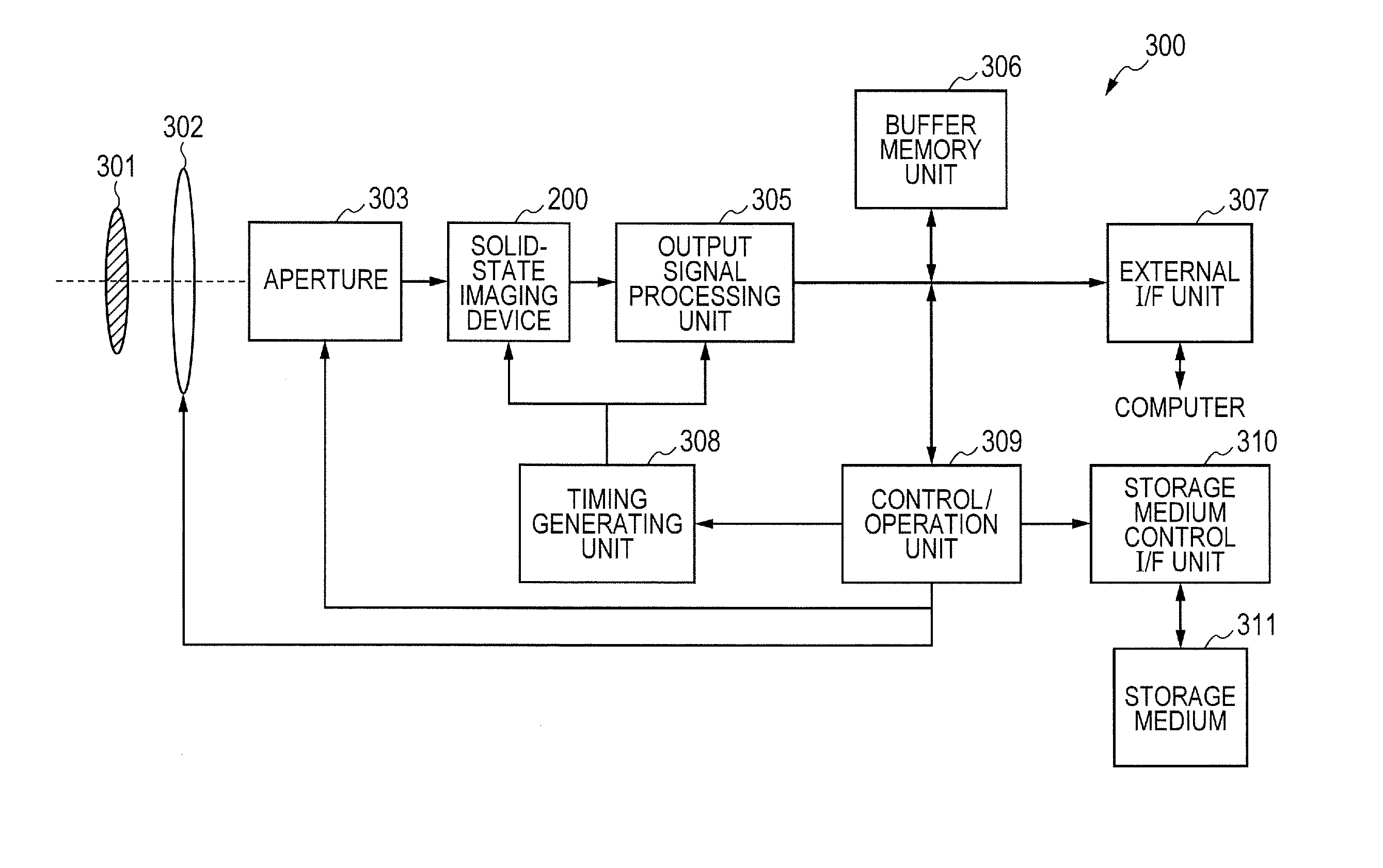
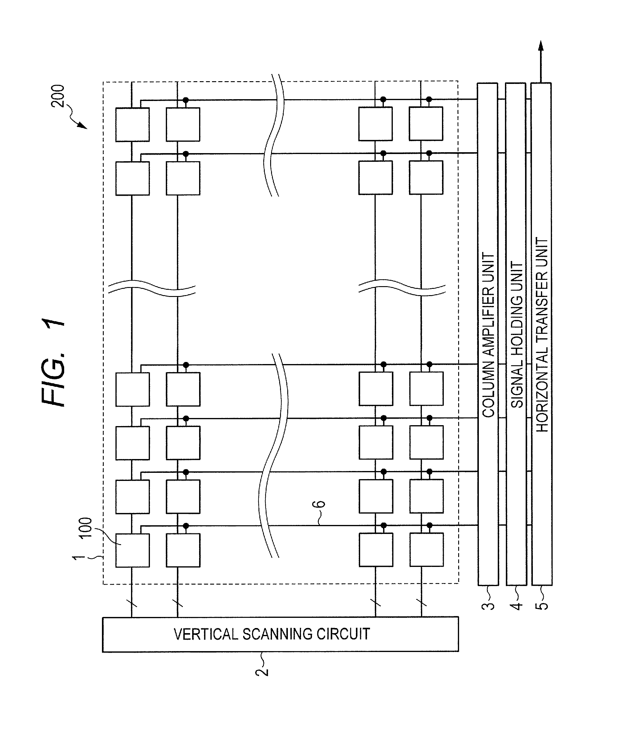
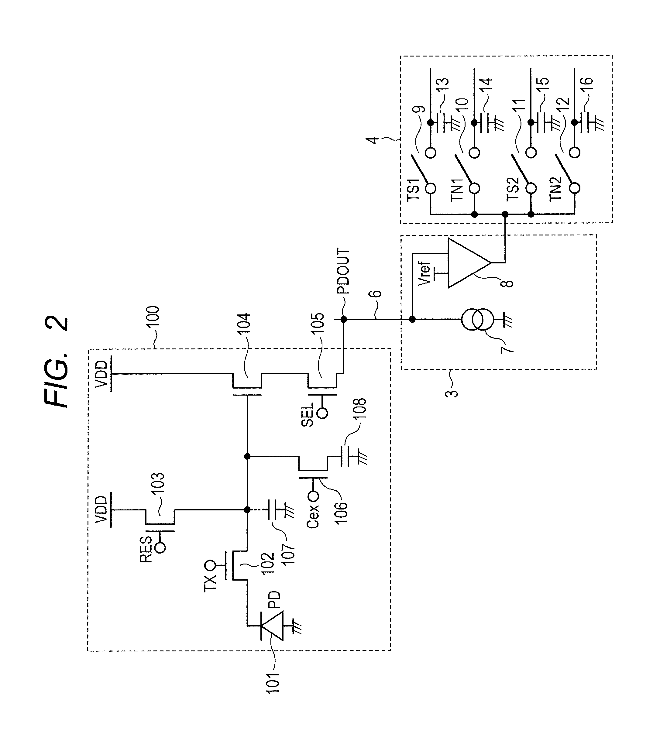
[0026]A solid-state imaging device and a method of driving the same according to a first embodiment of the present invention will be described with reference to FIG. 1 to FIG. 5.
[0027]FIG. 1 is a block diagram illustrating one example of the configuration of the solid-state imaging device according to the present embodiment. FIG. 2 is a circuit diagram illustrating one example of the configuration of the solid-state imaging device according to the present embodiment. FIG. 3 is a timing chart illustrating one example of the method of driving the solid-state imaging device according to the present embodiment. FIG. 4 is a graph illustrating the dependence with respect to an optical input amount of an output voltage in the solid-state imaging device according to the present embodiment. FIG. 5 is a graph illustrating the dependence with respect to an optical input amount of an output signal in the solid-state imaging device according to the present embodiment.
[0028]First, the structure o...
second embodiment
[0087]A solid-state imaging device and a method of driving the same according to a second embodiment of the present invention will be described with reference to FIG. 6 and FIG. 7. In FIG. 6 and FIG. 7, constituent elements that are the same as in the solid-state imaging device and the method of driving the same according to the first embodiment illustrated in FIG. 1 to FIG. 5 are denoted by the same reference characters as in FIG. 1 to FIG. 5, and a description of those constituent elements is omitted or abbreviated hereunder.
[0088]FIG. 6 is a circuit diagram illustrating an example of the configuration of the solid-state imaging device according to the present embodiment. FIG. 7 is a timing chart illustrating an example of a method of driving the solid-state imaging device according to the present embodiment.
[0089]In the solid-state imaging device according to the first embodiment the signal holding unit 4 is constituted by the four select switches 9, 10, 11 and 12 and the four si...
third embodiment
[0094]A solid-state imaging device and a method of driving the same according to a third embodiment of the present invention will be described with reference to FIG. 8 and FIG. 9. In FIG. 8 and FIG. 9, constituent elements that are the same as in the solid-state imaging device and the method of driving the same according to the first and second embodiments illustrated in FIG. 1 to FIG. 7 are denoted by the same reference characters as in FIG. 1 to FIG. 7, and a description of those constituent elements is omitted or abbreviated hereunder.
[0095]FIG. 8 is a circuit diagram illustrating an example of the configuration of the solid-state imaging device according to the present embodiment. FIG. 9 is a timing chart illustrating an example of a method of driving the solid-state imaging device according to the present embodiment.
[0096]As illustrated in FIG. 8, in the solid-state imaging device according to the present embodiment, the additional capacitor select transistor 106 and the additi...
PUM
 Abstract
Description
Claims
Application Information