Solid-state imaging device, driving method of solid-state imaging device, and electronic apparatus

Inactive Publication Date: 2011-10-06
SONY SEMICON SOLUTIONS CORP
View PDF2 Cites 36 Cited by
  • Summary
  • Abstract
  • Description
  • Claims
  • Application Information

AI Technical Summary

Benefits of technology

[0032]According to the first to third embodiments, the image quality of an image imaged using a global shutter is improved. In particular, according to the first embodiment of the invention, it is possible to expand dynamic range without lowering the image quality of an image imaged using the global shutter. Additionally, accord

Problems solved by technology

Conversely, unless the area of the photodiode for each pixel is made smaller, the area for each pixel becomes large and the size of the solid-state imaging device becomes large.
However, it is difficult to form a distribution of impurities in the photodiode so that it is possible to completely transfer electric charges in different directions from the one photodiode.
As a result, there is noise, variation in pixel characteristics, and the like, and deterioration in image quality is caused.
WO2007-83704, since performi

Method used


Image

  • Solid-state imaging device, driving method of solid-state imaging device, and electronic apparatus
  • Solid-state imaging device, driving method of solid-state imaging device, and electronic apparatus
  • Solid-state imaging device, driving method of solid-state imaging device, and electronic apparatus

Examples


Example

[0047]First, a first embodiment of the invention will be described with reference to FIGS. 1 to 7.

Configuration Example of Solid-state Imaging Device

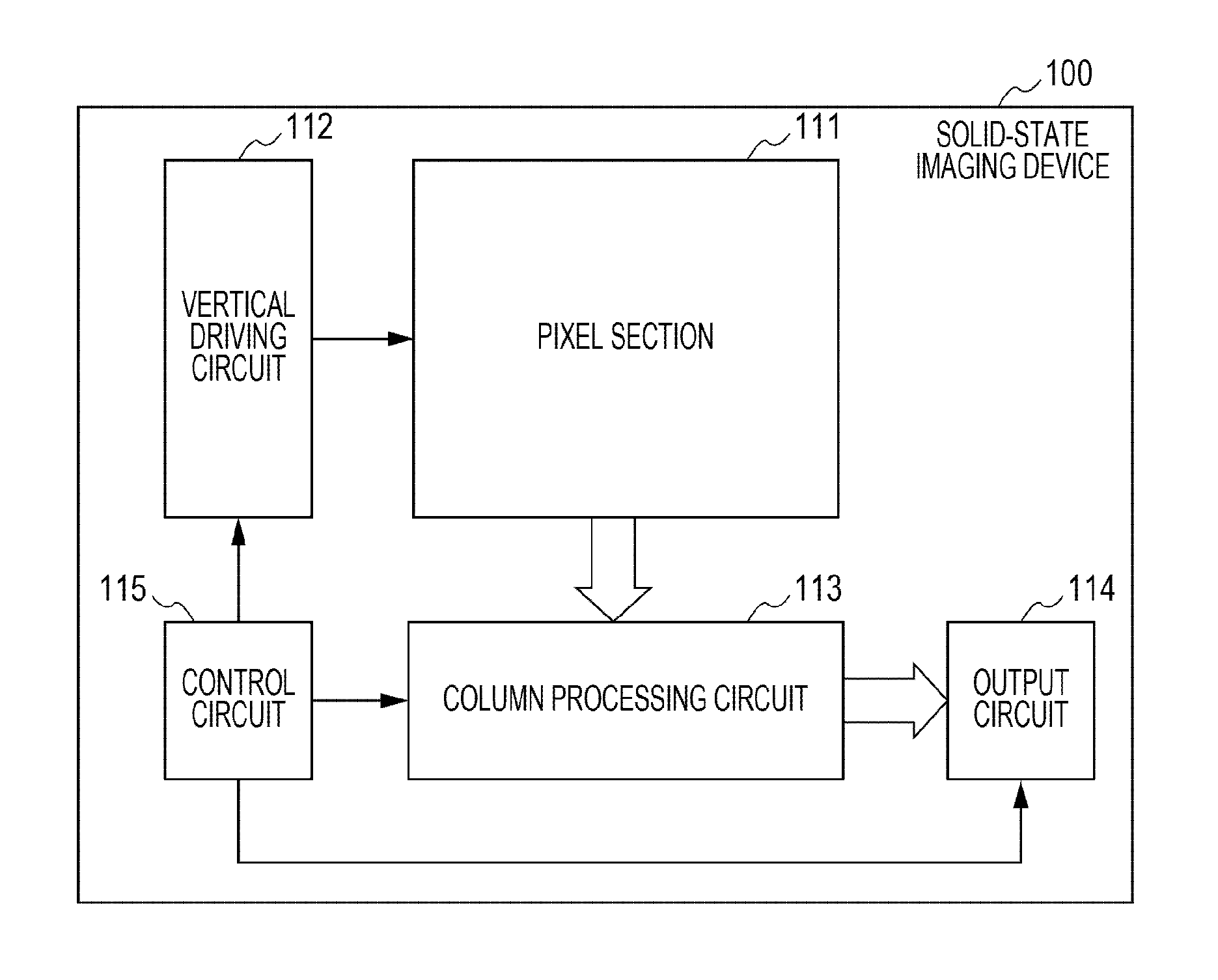
[0048]FIG. 1 is a block diagram illustrating a configuration example of a solid-state imaging device according to an embodiment of the invention.

[0049]A solid-state imaging device 100 is configured to include a pixel section 111, a vertical driving circuit 112, a column processing circuit 113, an output circuit 114, and a control circuit 115. The pixel section 111, the vertical driving circuit 112, the column processing circuit 113, the output circuit 114, and the control circuit 115 are formed on a semiconductor substrate (chip) which is not shown.

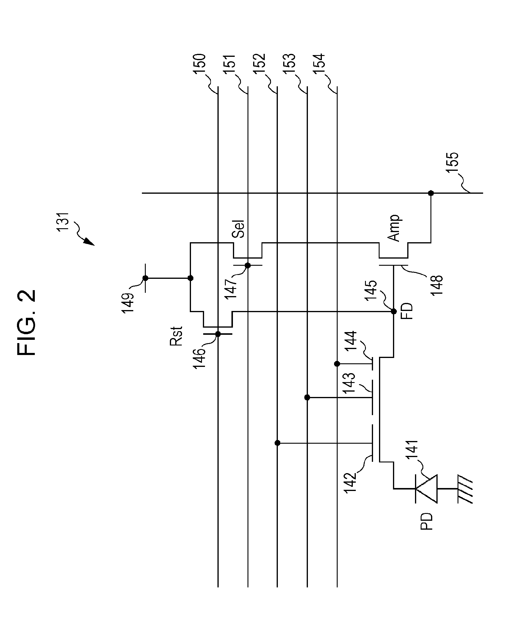
[0050]In the pixel section 111, the pixel units (the pixel units 131 of FIGS. 2 and 3), which have a photoelectric conversion element which generates and internally accumulates photoelectric charge with an electric charge amount corresponding to an amount of incident light, are arranged two-d...

Example

Second Embodiment of Driving Method of Unit Pixel 131

[0127]Next, a second embodiment of a driving method of the unit pixel 131 of the solid-state imaging device 100 will be described with reference to FIGS. 8 to 10. Here, FIG. 8 is a flow chart for describing the driving process of the unit pixel 131. In addition, FIG. 9 is a potential diagram of each section of the unit pixel 131. In the potential diagram of FIG. 9, the vertical axis shows potential and a downward direction means that potential with regard to electrons becomes lower (or higher). Furthermore, FIG. 10 is a timing chart for describing the driving process of the unit pixel 131. The horizontal direction of FIG. 10 shows time and the vertical direction shows the scanning direction.

[0128]In addition, in the second embodiment, there are two unit pixels 131; the unit pixel 131 where the next exposure is started before the signal electric charge is read out and the unit pixel 131 where the next exposure is started after the ...


PUM


Abstract

A solid-state imaging device with unit pixels which have a photoelectric conversion element, an electric charge transferring/accumulating unit with multiple levels able to transfer electric charge generated in the photoelectric conversion element and accumulate the electric charge, and an electric charge detection unit that holds the electric charge transferred from the photoelectric conversion element, where, after resetting the photoelectric conversion element, all unit pixels simultaneously transfer signal electric charges, which are generated in the photoelectric conversion element during continuous exposure times of which each has a different duration, to the electric charge transferring/accumulating units and accumulate the signal electric charges in the different respective electric charge transferring/accumulating units, and in units of one or more pixels, the signal electric charges is transferred to the electric charge detecting unit and a plurality of signals which respectively corresponds to the plurality of signal electric charges is read out.

Description

BACKGROUND OF THE INVENTION[0001]1. Field of the Invention[0002]The present invention relates to a solid-state imaging device, a driving method of the solid-state imaging device, and an electronic apparatus, and in particular, to a solid-state imaging device corresponding to a global shutter, a driving method of the solid-state imaging device, and an electronic apparatus.[0003]2. Description of the Related Art[0004]In the related art, it has been proposed that a dynamic range of a solid-state imaging device may be expanded by providing two potential wells with regard to one photodiode (for example, refer to International Publication No. WO2007-83704). Specifically, a potential well is provided on both sides of a photodiode so that there is a difference in an inflowing amount of electric charge with regard to light of the same intensity. Thus, it has been proposed that the electric charge that is accumulated in the potential well where the inflow amount is larger is read out as a hig...

Claims


Application Information

Patent Timeline
IPC IPC(8): H04N5/335
CPCH01L27/14609H01L27/14643H04N5/3745H04N5/35581H04N5/353H04N25/53H04N25/589H04N25/77
Inventor MABUCHI, KEIJI
Owner SONY SEMICON SOLUTIONS CORP
Why Eureka
Try Eureka