Semiconductor package and method of manufacturing the same

a technology of semiconductor and package, applied in the direction of semiconductor/solid-state device details, semiconductor devices, electrical apparatus, etc., can solve the problems of signal errors still exist, and it is not possible to eliminate electromagnetic interference caused by radio frequency chips

Active Publication Date: 2015-11-19
SILICONWARE PRECISION IND CO LTD
View PDF2 Cites 4 Cited by
  • Summary
  • Abstract
  • Description
  • Claims
  • Application Information

AI Technical Summary

Benefits of technology

[0014]In summary, in the semiconductor package and a method of manufacturing the same, the shielding member is disposed between at least two of

Problems solved by technology

However, although the outer portion of the conventional radio frequency module 1 can be protected through the metal thin film 14, it is no

Method used


Image

  • Semiconductor package and method of manufacturing the same
  • Semiconductor package and method of manufacturing the same
  • Semiconductor package and method of manufacturing the same

Examples


Embodiment Construction

[0018]The present invention is described in the following with specific embodiments, so that one skilled in the pertinent art can easily understand other advantages and effects of the present invention from the disclosure of the present invention.

[0019]It should be noted that all the drawings are not intended to limit the present invention. Various modification and variations can be made without departing from the spirit of the present invention. Further, terms, such as “top”, “one”, “bottom”, etc., are merely for illustrative purpose and should not be construed to limit the scope of the present invention.

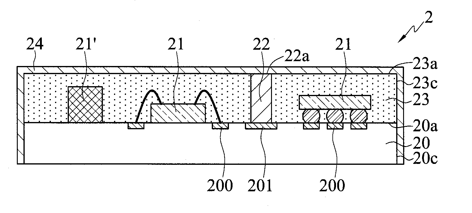
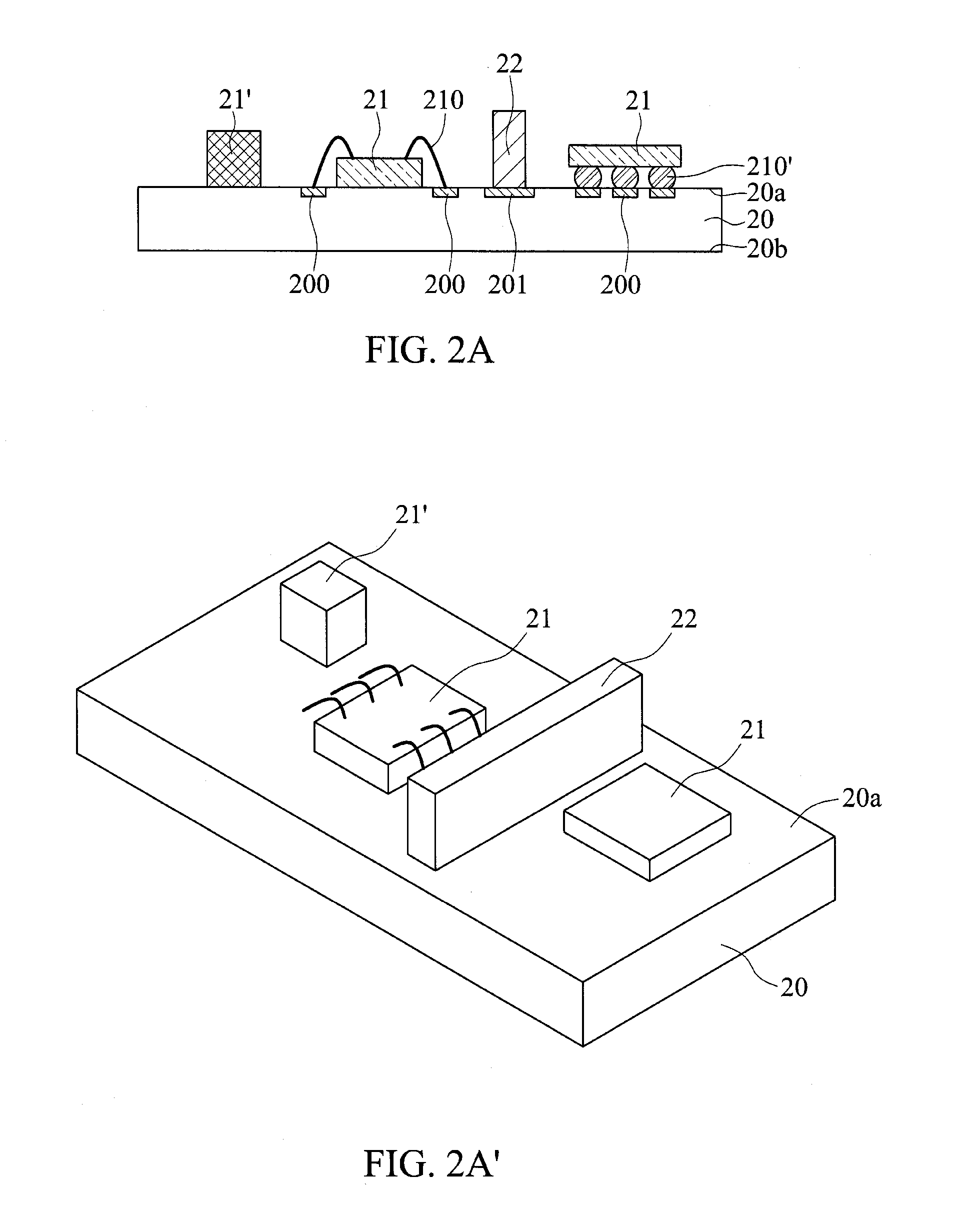
[0020]Referring to FIGS. 2A to 2C, a method of manufacturing a semiconductor package 2 is provided. In an embodiment, the semiconductor package 2 is an electromagnetic wave generator such as a radio frequency (RF) module.

[0021]As illustrated in FIGS. 2A and 2A′, a substrate 20 having a top surface 20a and a bottom surface 20b is provided, and a plurality of semiconductor elements 2...


PUM


Abstract

This invention provides a semiconductor package, including a substrate, a plurality of semiconductor elements disposed on the substrate, at least one shielding member disposed between at least two of the semiconductor elements, and an encapsulant encapsulating the semiconductor elements and shielding members. Through the shielding member, electromagnetic interference caused among semiconductor elements can be prevented.

Description

BACKGROUND OF THE INVENTION[0001]1. Field of the Invention[0002]The present invention relates to semiconductor packages, and, more particularly, to a semiconductor package and a method of manufacturing the same that will not be electromagnetically interfered by electronic elements in the semiconductor package.[0003]2. Description of Related Art[0004]With rapid advancement in the technology of electronic industry, semiconductor products have been developed in various types, in view of improving electrical performance. Hence several semiconductor types are incorporated with shielding effect to prevent electromagnetic interference (EMI).[0005]A radio frequency (RF) module 1 prevents EMI. As shown in FIGS. 1A-1C, the radio frequency module 1 is formed by electrically connecting a plurality of radio frequency chips 11a, 11b and non-radio frequency electronic elements 11 onto a substrate 10, encapsulating the radio frequency chips 11a, 11b and the non-radio frequency electronic elements 1...

Claims


Application Information

Patent Timeline
IPC IPC(8): H01L23/552H01L23/66H01L21/56
CPCH01L23/552H01L23/66H01L21/56H01L23/3121H01L24/13H01L24/16H01L24/48H01L24/49H01L2224/131H01L2224/16225H01L2224/48091H01L2224/48227H01L2224/49175H01L2924/1421H01L2924/15313H01L2924/19105H01L2924/3025H01L2924/00014H01L2924/014H01L2224/45099H01L2224/45015H01L2924/207
Inventor CHANG, CHO-HSINHSU, TSUNG-HSIENCHUNG, HSIN-LUNGCHU, TE-FANGCHEN, CHIA-YANG
Owner SILICONWARE PRECISION IND CO LTD
Why Eureka
Try Eureka